- 您现在的位置:买卖IC网 > PDF目录11782 > PIC10F322-I/P (Microchip Technology)IC MCU 8BIT 896B FLASH 8DIP PDF资料下载
参数资料
| 型号: | PIC10F322-I/P |
| 厂商: | Microchip Technology |
| 文件页数: | 18/210页 |
| 文件大小: | 0K |
| 描述: | IC MCU 8BIT 896B FLASH 8DIP |
| 产品培训模块: | 8-bit PIC® Microcontroller Portfolio |
| 标准包装: | 60 |
| 系列: | PIC® 10F |
| 核心处理器: | PIC |
| 芯体尺寸: | 8-位 |
| 速度: | 16MHz |
| 外围设备: | 欠压检测/复位,POR,PWM,WDT |
| 输入/输出数: | 3 |
| 程序存储器容量: | 896B(512 x 14) |
| 程序存储器类型: | 闪存 |
| RAM 容量: | 64 x 8 |
| 电压 - 电源 (Vcc/Vdd): | 2.3 V ~ 5.5 V |
| 数据转换器: | A/D 3x8b |
| 振荡器型: | 内部 |
| 工作温度: | -40°C ~ 85°C |
| 封装/外壳: | 8-DIP(0.300",7.62mm) |
| 包装: | 管件 |
第1页第2页第3页第4页第5页第6页第7页第8页第9页第10页第11页第12页第13页第14页第15页第16页第17页当前第18页第19页第20页第21页第22页第23页第24页第25页第26页第27页第28页第29页第30页第31页第32页第33页第34页第35页第36页第37页第38页第39页第40页第41页第42页第43页第44页第45页第46页第47页第48页第49页第50页第51页第52页第53页第54页第55页第56页第57页第58页第59页第60页第61页第62页第63页第64页第65页第66页第67页第68页第69页第70页第71页第72页第73页第74页第75页第76页第77页第78页第79页第80页第81页第82页第83页第84页第85页第86页第87页第88页第89页第90页第91页第92页第93页第94页第95页第96页第97页第98页第99页第100页第101页第102页第103页第104页第105页第106页第107页第108页第109页第110页第111页第112页第113页第114页第115页第116页第117页第118页第119页第120页第121页第122页第123页第124页第125页第126页第127页第128页第129页第130页第131页第132页第133页第134页第135页第136页第137页第138页第139页第140页第141页第142页第143页第144页第145页第146页第147页第148页第149页第150页第151页第152页第153页第154页第155页第156页第157页第158页第159页第160页第161页第162页第163页第164页第165页第166页第167页第168页第169页第170页第171页第172页第173页第174页第175页第176页第177页第178页第179页第180页第181页第182页第183页第184页第185页第186页第187页第188页第189页第190页第191页第192页第193页第194页第195页第196页第197页第198页第199页第200页第201页第202页第203页第204页第205页第206页第207页第208页第209页第210页
PIC10(L)F320/322
DS41585A-page 114
Preliminary
2011 Microchip Technology Inc.
19.1
CLCx Setup
Programming the CLCx module is performed by config-
uring the four stages in the logic signal flow. The four
stages are:
Data selection
Data gating
Logic function selection
Output polarity
Each stage is setup at run time by writing to the corre-
sponding CLCx Special Function Registers. This has
the added advantage of permitting logic reconfiguration
on-the-fly during program execution.
19.1.1
DATA SELECTION
There are eight signals available as inputs to the con-
figurable logic. Four 8-input multiplexers are used to
select the inputs to pass on to the next stage.
Data inputs are selected with the CLCxSEL0 and
CLCxSEL1 registers (Register 19-3 and Register 19-4,
respectively).
Data selection is through four multiplexers as indicated
on the left side of Figure 19-2. Data inputs in the figure
are identified by a generic numbered input name.
Table 19-1 correlates the generic input name to the
actual signal for each CLC module. The columns
labeled lcxd1 through lcxd4 indicate the MUX output for
the selected data input. D1S through D4S are
abbreviations for the MUX select input codes:
LCxD1S<2:0> through LCxD4S<2:0>, respectively.
Selecting a data input in a column excludes all other
inputs in that column.
19.1.2
DATA GATING
Outputs from the input multiplexers are directed to the
desired logic function input through the data gating
stage. Each data gate can direct any combination of the
four selected inputs.
The gate stage is more than just signal direction. The gate
can be configured to direct each input signal as inverted
or non-inverted data. Directed signals are ANDed
together in each gate. The output of each gate can be
inverted before going on to the logic function stage.
The gating is in essence a 1-to-4 input AND/NAND/OR/
NOR gate. When every input is inverted and the output
is inverted, the gate is an OR of all enabled data inputs.
When the inputs and output are not inverted, the gate
is an AND or all enabled inputs.
Table 19-2 summarizes the basic logic that can be
obtained in gate 1 by using the gate logic select bits.
The table shows the logic of four input variables, but
each gate can be configured to use less than four. If no
inputs are selected, the output will be zero or one,
depending on the gate output polarity bit.
It is possible (but not recommended) to select both the
true and negated values of an input. When this is done,
the gate output is zero, regardless of the other inputs,
but may emit logic glitches (transient-induced pulses). If
the output of the channel must be zero or one, the
recommended method is to set all gate bits to zero and
use the gate polarity bit to set the desired level.
Data gating is configured with the logic gate select
registers as follows:
Gate 1: CLCxGLS0 (Register 19-5)
Gate 2: CLCxGLS1 (Register 19-6)
Gate 3: CLCxGLS2 (Register 19-7)
Gate 4: CLCxGLS3 (Register 19-8)
Register number suffixes are different than the gate
numbers because other variations of this module have
multiple gate selections in the same register.
Data gating is indicated in the right side of Figure 19-2.
Only one gate is shown in detail. The remaining three
gates are configured identically with the exception that
the data enables correspond to the enables for that gate.
Note:
Data selections are undefined at power-up.
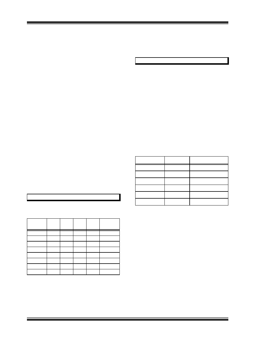
TABLE 19-1:
CLCx DATA INPUT
SELECTION
Data Input
lcxd1
D1S
lcxd2
D2S
lcxd3
D3S
lcxd4
D4S
CLC 1
CLCxIN[0]
000
CLCx
CLCxIN[1]
001
CLCxIN1
CLCxIN[2]
010
CLCxIN2
CLCxIN[3]
011
PWM1
CLCxIN[4]
100
PWM2
CLCxIN[5]
101
NCOx
CLCxIN[6]
110
FOSC
CLCxIN[7]
111
LFINTOSC
Note:
Data gating is undefined at power-up.
TABLE 19-2:
DATA GATING LOGIC
CLCxGLS0
LCxGyPOL
Gate Logic
0x55
1
AND
0x55
0
NAND
0xAA
1
NOR
0xAA
0
OR
0x00
0
Logic 0
0x00
1
Logic 1
相关PDF资料 |
PDF描述 |
|---|---|
| PIC12F1501-E/P | IC MCU 8BIT 1.75KB FLASH 8PDIP |
| PIC10F220-I/MC | IC PIC MCU FLASH 256X12 8DFN |
| PIC10F204-I/P | IC PIC MCU FLASH 256X12 8DIP |
| DS33X11+ | IC MAPPING ETHERNET 144CSBGA |
| V110B8H150BL2 | CONVERTER MOD DC/DC 8V 150W |
相关代理商/技术参数 |
参数描述 |
|---|---|
| PIC10F322T-E/OT | 制造商:Microchip Technology Inc 功能描述:896 B FLASH, 64 B RAM, 4 I/O, 8BIT ADC, PWM, CLC, DDS, CWG, - Tape and Reel 制造商:Microchip Technology Inc 功能描述:IC MCU 8BIT 896 B FLASH 6SOT23 制造商:Microchip Technology Inc 功能描述:896 B Flash, 64 B RAM, 4 I/O, 8bit ADC, PWM, CLC, NCO, CWG, TEMP Indicator, 2.3V |
| PIC10F322T-I/MC | 功能描述:8位微控制器 -MCU 448B FL 32B RAM 4I/O 8bit ADC 2.3-5.5V RoHS:否 制造商:Silicon Labs 核心:8051 处理器系列:C8051F39x 数据总线宽度:8 bit 最大时钟频率:50 MHz 程序存储器大小:16 KB 数据 RAM 大小:1 KB 片上 ADC:Yes 工作电源电压:1.8 V to 3.6 V 工作温度范围:- 40 C to + 105 C 封装 / 箱体:QFN-20 安装风格:SMD/SMT |
| PIC10F322T-I/MC | 制造商:Microchip Technology Inc 功能描述:896 B Flash 64 B RAM 4 I/O 8bit ADC |
| PIC10F322T-I/OT | 功能描述:8位微控制器 -MCU 448B FL 32B RAM 4I/O 8bit ADC 2.3-5.5V RoHS:否 制造商:Silicon Labs 核心:8051 处理器系列:C8051F39x 数据总线宽度:8 bit 最大时钟频率:50 MHz 程序存储器大小:16 KB 数据 RAM 大小:1 KB 片上 ADC:Yes 工作电源电压:1.8 V to 3.6 V 工作温度范围:- 40 C to + 105 C 封装 / 箱体:QFN-20 安装风格:SMD/SMT |
| PIC10FPROMOKIT | 制造商:Microchip Technology Inc 功能描述:STARTER KIT PIC10F WITH PICKIT1 |
发布紧急采购,3分钟左右您将得到回复。