- 您现在的位置:买卖IC网 > PDF目录11632 > PIC12F519-E/SN (Microchip Technology)IC PIC MCU FLASH 1KX12 8SOIC PDF资料下载
参数资料
| 型号: | PIC12F519-E/SN |
| 厂商: | Microchip Technology |
| 文件页数: | 46/96页 |
| 文件大小: | 0K |
| 描述: | IC PIC MCU FLASH 1KX12 8SOIC |
| 产品培训模块: | Asynchronous Stimulus |
| 标准包装: | 100 |
| 系列: | PIC® 12F |
| 核心处理器: | PIC |
| 芯体尺寸: | 8-位 |
| 速度: | 8MHz |
| 外围设备: | POR,WDT |
| 输入/输出数: | 5 |
| 程序存储器容量: | 1.5KB(1K x 12) |
| 程序存储器类型: | 闪存 |
| RAM 容量: | 41 x 8 |
| 电压 - 电源 (Vcc/Vdd): | 2 V ~ 5.5 V |
| 振荡器型: | 内部 |
| 工作温度: | -40°C ~ 125°C |
| 封装/外壳: | 8-SOIC(0.154",3.90mm 宽) |
| 包装: | 管件 |
第1页第2页第3页第4页第5页第6页第7页第8页第9页第10页第11页第12页第13页第14页第15页第16页第17页第18页第19页第20页第21页第22页第23页第24页第25页第26页第27页第28页第29页第30页第31页第32页第33页第34页第35页第36页第37页第38页第39页第40页第41页第42页第43页第44页第45页当前第46页第47页第48页第49页第50页第51页第52页第53页第54页第55页第56页第57页第58页第59页第60页第61页第62页第63页第64页第65页第66页第67页第68页第69页第70页第71页第72页第73页第74页第75页第76页第77页第78页第79页第80页第81页第82页第83页第84页第85页第86页第87页第88页第89页第90页第91页第92页第93页第94页第95页第96页
PIC12F519
DS41319B-page 48
2008 Microchip Technology Inc.
8.9
Program Verification/Code
Protection
If the code protection bits have not been programmed,
the on-chip program and data memory can be read out
for verification purposes.
The first 64 locations and the last location (OSCCAL)
can be read, regardless of the setting of the program
memory’s code protection bit. If the code protect bit
specific to the FLASH data memory is programmed,
then none of the contents of this memory region can be
verified externally.
8.10
ID Locations
Four memory locations are designated as ID locations
where users can store checksum or other code
identification numbers. These locations are not
accessible during normal execution, but are readable
and writable during program/verify.
Use only the lower 4 bits of the ID locations. The upper
bits should be programmed as 0s.
8.11
In-Circuit Serial Programming
The PIC12F519 device can be serially programmed
while in the end application circuit. This is simply done
with two lines for clock and data, and three other lines
for power, ground and the programming voltage. This
allows
users
to
manufacture
boards
with
unprogrammed PIC12F519 device and then program
the PIC12F519 device just before shipping the product.
This also allows the most recent firmware, or a custom
firmware, to be programmed.
The PIC12F519 device is placed into a Program/Verify
mode by holding the GP1 and GP0 pins low while
raising the MCLR (VPP) pin from VIL to VIHH (see
programming specification). The GP1 pin becomes the
programming clock, and the GP0 pin becomes the
programming data. Both GP1 and GP0 pins are Schmitt
Trigger inputs in this mode.
After Reset, a 6-bit command is then supplied to the
device. Depending on the command, 14 bits of program
data are then supplied to or from the device, depending
if the command was a Load or a Read. For complete
details of serial programming, please refer to the
“PIC12F519 Memory Programming Specification,”
(DS41316).
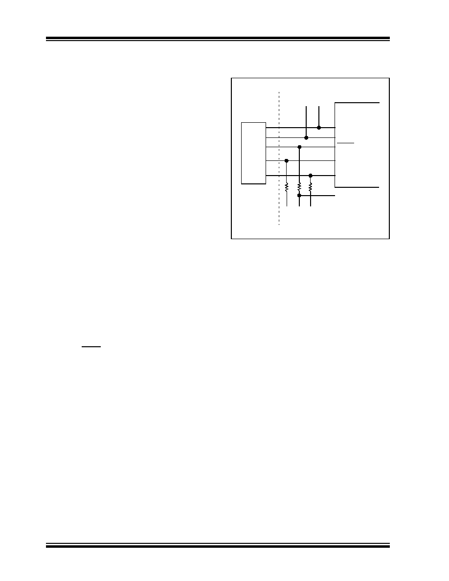
A typical In-Circuit Serial Programming connection is
shown in Figure 8-12.
FIGURE 8-12:
TYPICAL IN-CIRCUIT
SERIAL PROGRAMMING
CONNECTION
External
Connector
Signals
To Normal
Connections
To Normal
Connections
PIC12F519
VDD
VSS
MCLR/VPP
GP1/ICSPCLK
GP0/ICSPDAT
+5V
0V
VPP
CLK
Data
VDD
相关PDF资料 |
PDF描述 |
|---|---|
| VI-BWK-IX-F4 | CONVERTER MOD DC/DC 40V 75W |
| VI-BWK-IW-F1 | CONVERTER MOD DC/DC 40V 100W |
| 1-5413588-0 | CONN PLUG BNC AT&T735A R/A CRIMP |
| PIC12F509T-I/MC | IC PIC MCU FLASH 1024X12 8DFN |
| 1-413588-0 | CONN PLUG BNC AT&T735A R/A CRIMP |
相关代理商/技术参数 |
参数描述 |
|---|---|
| PIC12F519-I/MC | 功能描述:8位微控制器 -MCU 15KB Flash Prgrm 64B 8MHz Intrnl Oscilatr RoHS:否 制造商:Silicon Labs 核心:8051 处理器系列:C8051F39x 数据总线宽度:8 bit 最大时钟频率:50 MHz 程序存储器大小:16 KB 数据 RAM 大小:1 KB 片上 ADC:Yes 工作电源电压:1.8 V to 3.6 V 工作温度范围:- 40 C to + 105 C 封装 / 箱体:QFN-20 安装风格:SMD/SMT |
| PIC12F519-I/MS | 功能描述:8位微控制器 -MCU 15KB Flash Prgrm 64B 8MHz Intrnl Oscilatr RoHS:否 制造商:Silicon Labs 核心:8051 处理器系列:C8051F39x 数据总线宽度:8 bit 最大时钟频率:50 MHz 程序存储器大小:16 KB 数据 RAM 大小:1 KB 片上 ADC:Yes 工作电源电压:1.8 V to 3.6 V 工作温度范围:- 40 C to + 105 C 封装 / 箱体:QFN-20 安装风格:SMD/SMT |
| PIC12F519-I/P | 功能描述:8位微控制器 -MCU 8MHz Intrnl Oscilatr 1.5KB 64B Flash Data RoHS:否 制造商:Silicon Labs 核心:8051 处理器系列:C8051F39x 数据总线宽度:8 bit 最大时钟频率:50 MHz 程序存储器大小:16 KB 数据 RAM 大小:1 KB 片上 ADC:Yes 工作电源电压:1.8 V to 3.6 V 工作温度范围:- 40 C to + 105 C 封装 / 箱体:QFN-20 安装风格:SMD/SMT |
| PIC12F519-I/SN | 功能描述:8位微控制器 -MCU 1.5KB Flash Program 64B FData 8MHz Osc RoHS:否 制造商:Silicon Labs 核心:8051 处理器系列:C8051F39x 数据总线宽度:8 bit 最大时钟频率:50 MHz 程序存储器大小:16 KB 数据 RAM 大小:1 KB 片上 ADC:Yes 工作电源电压:1.8 V to 3.6 V 工作温度范围:- 40 C to + 105 C 封装 / 箱体:QFN-20 安装风格:SMD/SMT |
| PIC12F519T-E/MC | 制造商:MICROCHIP 制造商全称:Microchip Technology 功能描述:8-Pin, 8-Bit Flash Microcontroller |
发布紧急采购,3分钟左右您将得到回复。