- 您现在的位置:买卖IC网 > PDF目录11541 > PIC12F675-I/MD (Microchip Technology)IC PIC MCU FLASH 1KX14 8DFN PDF资料下载
参数资料
| 型号: | PIC12F675-I/MD |
| 厂商: | Microchip Technology |
| 文件页数: | 14/35页 |
| 文件大小: | 0K |
| 描述: | IC PIC MCU FLASH 1KX14 8DFN |
| 产品培训模块: | Asynchronous Stimulus 8-bit PIC® Microcontroller Portfolio |
| 标准包装: | 91 |
| 系列: | PIC® 12F |
| 核心处理器: | PIC |
| 芯体尺寸: | 8-位 |
| 速度: | 20MHz |
| 外围设备: | POR,WDT |
| 输入/输出数: | 5 |
| 程序存储器容量: | 1.75KB(1K x 14) |
| 程序存储器类型: | 闪存 |
| EEPROM 大小: | 128 x 8 |
| RAM 容量: | 64 x 8 |
| 电压 - 电源 (Vcc/Vdd): | 2 V ~ 5.5 V |
| 数据转换器: | A/D 4x10b |
| 振荡器型: | 内部 |
| 工作温度: | -40°C ~ 85°C |
| 封装/外壳: | 8-VDFN 裸露焊盘 |
| 包装: | 管件 |
| 产品目录页面: | 637 (CN2011-ZH PDF) |
| 配用: | AC164326-ND - MODULA SKT PM3 20QFN |
第1页第2页第3页第4页第5页第6页第7页第8页第9页第10页第11页第12页第13页当前第14页第15页第16页第17页第18页第19页第20页第21页第22页第23页第24页第25页第26页第27页第28页第29页第30页第31页第32页第33页第34页第35页
21
0787E–MICRO–3/06
AT89S53
.
Notes:
1. “h” = weakly pulled “High” internally.
2. Chip Erase and Serial Programming Fuse require a 10 ms PROG pulse. Chip Erase needs to be performed first before
reprogramming any byte with a content other than FFH.
3. P3.4 is pulled Low during programming to indicate RDY/BSY.
4. “X” = don’t care
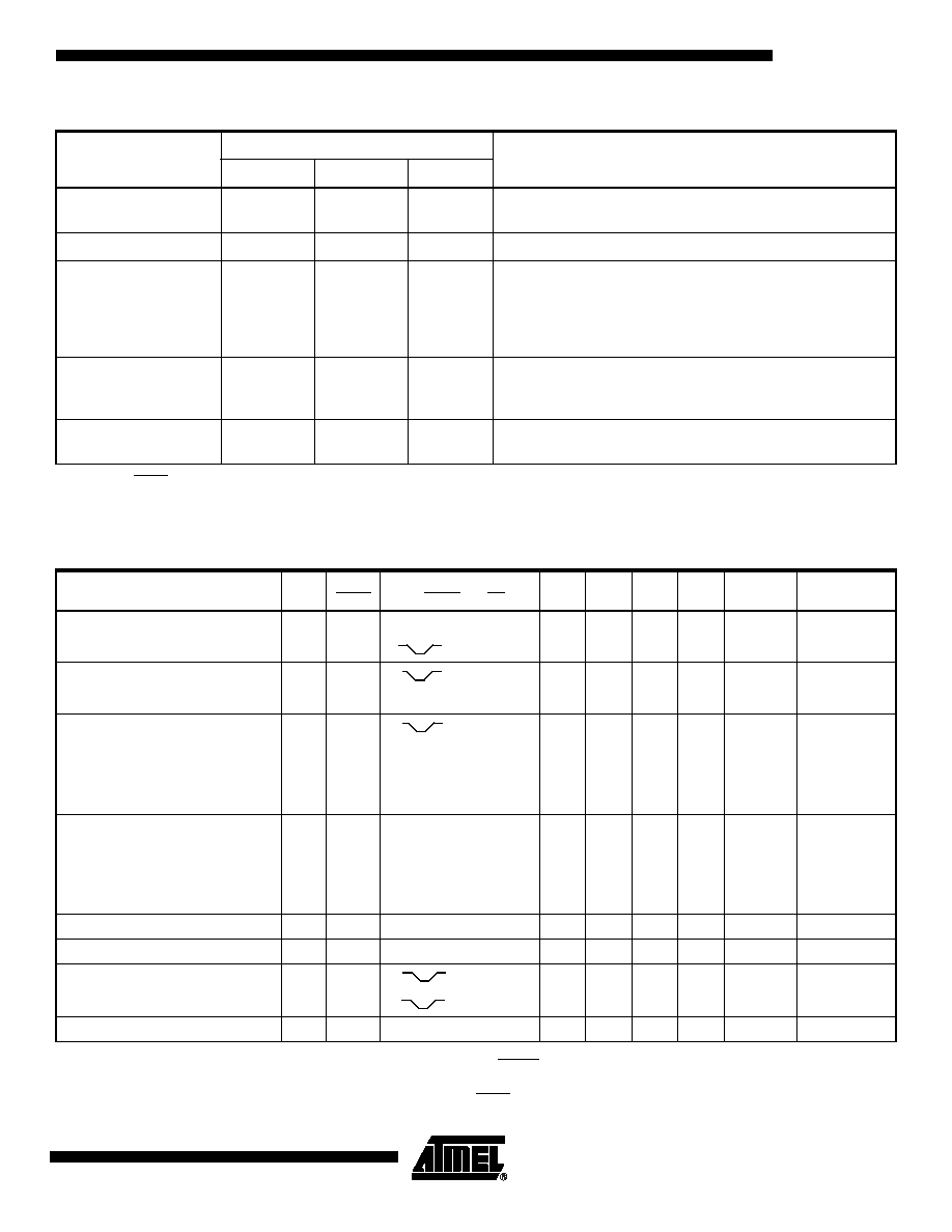
Flash Parallel Programming Modes
Mode
RST
PSEN
ALE/PROG
EA/V
PP
P2.6
P2.7
P3.6
P3.7
Data I/O
P0.7:0
Address
P2.5:0 P1.7:0
Serial Prog. Modes
H
x
Chip Erase
H
L
12V
H
L
X
Write (12K bytes) Memory
H
L
12V
L
H
DIN
ADDR
Read (12K bytes) Memory
H
L
H
12V
L
H
DOUT
ADDR
Write Lock Bits:
H
L
12V
H
L
H
L
DIN
X
Bit - 1
P0.7 = 0
X
Bit - 2
P0.6 = 0
X
Bit - 3
P0.5 = 0
X
Read Lock Bits:
H
L
H
12V
H
L
DOUT
X
Bit - 1
@P0.2
X
Bit - 2
@P0.1
X
Bit - 3
@P0.0
X
Read Atmel Code
H
L
H
12V
L
DOUT
30H
Read Device Code
H
L
H
12V
L
DOUT
31H
Serial Prog. Enable
H
L
12V
L
H
L
H
P0.0 = 0
X
Serial Prog. Disable
H
L
12V
L
H
L
H
P0.0 = 1
X
Read Serial Prog. Fuse
H
L
H
12V
H
L
H
@P0.0
X
(2)
Instruction Set
Notes:
1. DATA polling is used to indicate the end of a write cycle which typically takes less than 10 ms at 2.7V.
2. “x” = don’t care.
Instruction
Input Format
Operation
Byte 1
Byte 2
Byte 3
Programming Enable
1010 1100
0101 0011
xxxx xxxx
Enable serial programming interface after RST goes
high.
Chip Erase
1010 1100
xxxx x100
xxxx xxxx
Chip erase the 12K memory array.
Read Code Memory
low addr
xxxx xxxx
Read data from Code memory array at the selected
address. The 6 MSBs of the first byte are the high order
address bits. The low order address bits are in the
second byte. Data are available at pin MISO during the
third byte.
Write Code Memory
low addr
data in
Write data to Code memory location at selected
address. The address bits are the 6 MSBs of the first
byte together with the second byte.
Write Lock Bits
1010 1100
xxxx xxxx
Write lock bits.
Set LB1, LB2 or LB3 = “0” to program lock bits.
A12 A11
A10
A9
A8
A13
01
A12 A11
A10
A9
A8
A13
10
LB1 LB2
LB3
xx111
相关PDF资料 |
PDF描述 |
|---|---|
| VI-21M-IY-B1 | CONVERTER MOD DC/DC 10V 50W |
| VI-B1R-IY-B1 | CONVERTER MOD DC/DC 7.5V 50W |
| VE-J1N-IX-S | CONVERTER MOD DC/DC 18.5V 75W |
| VI-21R-IY-B1 | CONVERTER MOD DC/DC 7.5V 50W |
| VE-B1R-IY-B1 | CONVERTER MOD DC/DC 7.5V 50W |
相关代理商/技术参数 |
参数描述 |
|---|---|
| PIC12F675-IMF | 制造商:MICROCHIP 制造商全称:Microchip Technology 功能描述:8-Pin, Flash-Based 8-Bit CMOS Microcontrollers |
| PIC12F675-IP | 制造商:MICROCHIP 制造商全称:Microchip Technology 功能描述:8-Pin, Flash-Based 8-Bit CMOS Microcontrollers |
| PIC12F675-ISN | 制造商:MICROCHIP 制造商全称:Microchip Technology 功能描述:8-Pin, Flash-Based 8-Bit CMOS Microcontrollers |
| PIC12F675T-E/MD | 制造商:MICROCHIP 制造商全称:Microchip Technology 功能描述:8-Pin, Flash-Based 8-Bit CMOS Microcontrollers |
| PIC12F675T-E/MF | 功能描述:8位微控制器 -MCU 1.75KB 64 RAM 6 I/O Ext Temp DFN8 RoHS:否 制造商:Silicon Labs 核心:8051 处理器系列:C8051F39x 数据总线宽度:8 bit 最大时钟频率:50 MHz 程序存储器大小:16 KB 数据 RAM 大小:1 KB 片上 ADC:Yes 工作电源电压:1.8 V to 3.6 V 工作温度范围:- 40 C to + 105 C 封装 / 箱体:QFN-20 安装风格:SMD/SMT |
发布紧急采购,3分钟左右您将得到回复。