- 您现在的位置:买卖IC网 > PDF目录11779 > PIC12F752-I/MF (Microchip Technology)IC MCU 8BIT 1024B FLASH 8-DFN PDF资料下载
参数资料
| 型号: | PIC12F752-I/MF |
| 厂商: | Microchip Technology |
| 文件页数: | 8/201页 |
| 文件大小: | 0K |
| 描述: | IC MCU 8BIT 1024B FLASH 8-DFN |
| 标准包装: | 120 |
| 系列: | PIC® 12F |
| 核心处理器: | PIC |
| 芯体尺寸: | 8-位 |
| 速度: | 20MHz |
| 外围设备: | 欠压检测/复位,POR,PWM,WDT |
| 输入/输出数: | 5 |
| 程序存储器容量: | 1.75KB(1K x 14) |
| 程序存储器类型: | 闪存 |
| RAM 容量: | 64 x 8 |
| 电压 - 电源 (Vcc/Vdd): | 2 V ~ 5.5 V |
| 数据转换器: | A/D 4x10b |
| 振荡器型: | 内部 |
| 工作温度: | -40°C ~ 85°C |
| 封装/外壳: | 8-VDFN 裸露焊盘 |
| 包装: | 管件 |
第1页第2页第3页第4页第5页第6页第7页当前第8页第9页第10页第11页第12页第13页第14页第15页第16页第17页第18页第19页第20页第21页第22页第23页第24页第25页第26页第27页第28页第29页第30页第31页第32页第33页第34页第35页第36页第37页第38页第39页第40页第41页第42页第43页第44页第45页第46页第47页第48页第49页第50页第51页第52页第53页第54页第55页第56页第57页第58页第59页第60页第61页第62页第63页第64页第65页第66页第67页第68页第69页第70页第71页第72页第73页第74页第75页第76页第77页第78页第79页第80页第81页第82页第83页第84页第85页第86页第87页第88页第89页第90页第91页第92页第93页第94页第95页第96页第97页第98页第99页第100页第101页第102页第103页第104页第105页第106页第107页第108页第109页第110页第111页第112页第113页第114页第115页第116页第117页第118页第119页第120页第121页第122页第123页第124页第125页第126页第127页第128页第129页第130页第131页第132页第133页第134页第135页第136页第137页第138页第139页第140页第141页第142页第143页第144页第145页第146页第147页第148页第149页第150页第151页第152页第153页第154页第155页第156页第157页第158页第159页第160页第161页第162页第163页第164页第165页第166页第167页第168页第169页第170页第171页第172页第173页第174页第175页第176页第177页第178页第179页第180页第181页第182页第183页第184页第185页第186页第187页第188页第189页第190页第191页第192页第193页第194页第195页第196页第197页第198页第199页第200页第201页
105
7682C–AUTO–04/08
AT90CAN32/64/128
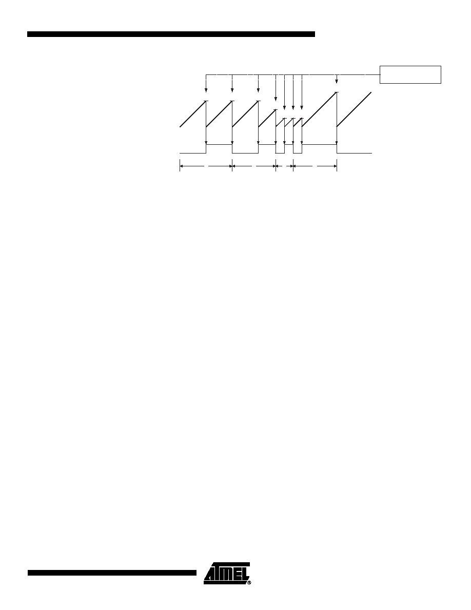
Figure 12-5. CTC Mode, Timing Diagram
An interrupt can be generated each time the counter value reaches the TOP value by using the
OCF0A flag. If the interrupt is enabled, the interrupt handler routine can be used for updating the
TOP value. However, changing TOP to a value close to BOTTOM when the counter is running
with none or a low prescaler value must be done with care since the CTC mode does not have
the double buffering feature. If the new value written to OCR0A is lower than the current value of
TCNT0, the counter will miss the compare match. The counter will then have to count to its max-
imum value (0xFF) and wrap around starting at 0x00 before the compare match can occur.
For generating a waveform output in CTC mode, the OC0A output can be set to toggle its logical
level on each compare match by setting the Compare Output mode bits to toggle mode
(COM0A1:0 = 1). The OC0A value will not be visible on the port pin unless the data direction for
the pin is set to output. The waveform generated will have a maximum frequency of fOC0A =
fclk_I/O/2 when OCR0A is set to zero (0x00). The waveform frequency is defined by the following
equation:
The N variable represents the prescale factor (1, 8, 64, 256, or 1024).
As for the Normal mode of operation, the TOV0 flag is set in the same timer clock cycle that the
counter counts from MAX to 0x00.
12.7.3
Fast PWM Mode
The fast Pulse Width Modulation or fast PWM mode (WGM01:0 = 3) provides a high frequency
PWM waveform generation option. The fast PWM differs from the other PWM option by its sin-
gle-slope operation. The counter counts from BOTTOM to MAX then restarts from BOTTOM. In
non-inverting Compare Output mode, the Output Compare (OC0A) is cleared on the compare
match between TCNT0 and OCR0A, and set at BOTTOM. In inverting Compare Output mode,
the output is set on compare match and cleared at BOTTOM. Due to the single-slope operation,
the operating frequency of the fast PWM mode can be twice as high as the phase correct PWM
mode that use dual-slope operation. This high frequency makes the fast PWM mode well suited
for power regulation, rectification, and DAC applications. High frequency allows physically small
sized external components (coils, capacitors), and therefore reduces total system cost.
In fast PWM mode, the counter is incremented until the counter value matches the MAX value.
The counter is then cleared at the following timer clock cycle. The timing diagram for the fast
PWM mode is shown in Figure 12-6. The TCNT0 value is in the timing diagram shown as a his-
togram for illustrating the single-slope operation. The diagram includes non-inverted and
TCNTn
OCnx
(Toggle)
OCnx Interrupt Flag S
1
4
Period
2
3
(COMnx1:0 = 1)
f
OC nx
fclk_I/O
2 N
1
OCRnx
+
(
)
--------------------------------------------------
=
相关PDF资料 |
PDF描述 |
|---|---|
| PIC16F1503-I/P | MCU 8BIT 3.5KB FLASH 14PDIP |
| VE-B4N-IW-F1 | CONVERTER MOD DC/DC 18.5V 100W |
| VE-B4M-IX-F1 | CONVERTER MOD DC/DC 10V 75W |
| PIC16LF1503-I/P | MCU 8BIT 3.5KB FLASH 14PDIP |
| MS27473E14B35SC | CONN PLUG 37POS STRAIGHT W/SCKT |
相关代理商/技术参数 |
参数描述 |
|---|---|
| PIC12F752-I-SN | 制造商:MICROCHIP 制造商全称:Microchip Technology 功能描述:8-Pin, Flash-Based 8-Bit CMOS Microcontrollers |
| PIC12F752T-I/MF | 功能描述:8位微控制器 -MCU 1.75KB 64BRAM 6 I/O 8MHz Int Osc 5MIPS RoHS:否 制造商:Silicon Labs 核心:8051 处理器系列:C8051F39x 数据总线宽度:8 bit 最大时钟频率:50 MHz 程序存储器大小:16 KB 数据 RAM 大小:1 KB 片上 ADC:Yes 工作电源电压:1.8 V to 3.6 V 工作温度范围:- 40 C to + 105 C 封装 / 箱体:QFN-20 安装风格:SMD/SMT |
| PIC12F752T-I/SN | 功能描述:8位微控制器 -MCU 1.75KB 64BRAM 6 I/O 8MHz Int Osc 5MIPS RoHS:否 制造商:Silicon Labs 核心:8051 处理器系列:C8051F39x 数据总线宽度:8 bit 最大时钟频率:50 MHz 程序存储器大小:16 KB 数据 RAM 大小:1 KB 片上 ADC:Yes 工作电源电压:1.8 V to 3.6 V 工作温度范围:- 40 C to + 105 C 封装 / 箱体:QFN-20 安装风格:SMD/SMT |
| PIC12HV609-E/MD | 功能描述:8位微控制器 -MCU 1.75KB Flash, E TEMP 64B RAM, DFN8 RoHS:否 制造商:Silicon Labs 核心:8051 处理器系列:C8051F39x 数据总线宽度:8 bit 最大时钟频率:50 MHz 程序存储器大小:16 KB 数据 RAM 大小:1 KB 片上 ADC:Yes 工作电源电压:1.8 V to 3.6 V 工作温度范围:- 40 C to + 105 C 封装 / 箱体:QFN-20 安装风格:SMD/SMT |
| PIC12HV609-E/MF | 功能描述:8位微控制器 -MCU 1.75KB Flash 64B RAM 6 I/O 8MHz INT OSC RoHS:否 制造商:Silicon Labs 核心:8051 处理器系列:C8051F39x 数据总线宽度:8 bit 最大时钟频率:50 MHz 程序存储器大小:16 KB 数据 RAM 大小:1 KB 片上 ADC:Yes 工作电源电压:1.8 V to 3.6 V 工作温度范围:- 40 C to + 105 C 封装 / 箱体:QFN-20 安装风格:SMD/SMT |
发布紧急采购,3分钟左右您将得到回复。