- 您现在的位置:买卖IC网 > PDF目录11779 > PIC12F752-I/P (Microchip Technology)IC MCU 8BIT 1024B FLASH 8-PDIP PDF资料下载
参数资料
| 型号: | PIC12F752-I/P |
| 厂商: | Microchip Technology |
| 文件页数: | 99/201页 |
| 文件大小: | 0K |
| 描述: | IC MCU 8BIT 1024B FLASH 8-PDIP |
| 标准包装: | 60 |
| 系列: | PIC® 12F |
| 核心处理器: | PIC |
| 芯体尺寸: | 8-位 |
| 速度: | 20MHz |
| 外围设备: | 欠压检测/复位,POR,PWM,WDT |
| 输入/输出数: | 5 |
| 程序存储器容量: | 1.75KB(1K x 14) |
| 程序存储器类型: | 闪存 |
| RAM 容量: | 64 x 8 |
| 电压 - 电源 (Vcc/Vdd): | 2 V ~ 5.5 V |
| 数据转换器: | A/D 4x10b |
| 振荡器型: | 内部 |
| 工作温度: | -40°C ~ 85°C |
| 封装/外壳: | 8-DIP(0.300",7.62mm) |
| 包装: | 管件 |
第1页第2页第3页第4页第5页第6页第7页第8页第9页第10页第11页第12页第13页第14页第15页第16页第17页第18页第19页第20页第21页第22页第23页第24页第25页第26页第27页第28页第29页第30页第31页第32页第33页第34页第35页第36页第37页第38页第39页第40页第41页第42页第43页第44页第45页第46页第47页第48页第49页第50页第51页第52页第53页第54页第55页第56页第57页第58页第59页第60页第61页第62页第63页第64页第65页第66页第67页第68页第69页第70页第71页第72页第73页第74页第75页第76页第77页第78页第79页第80页第81页第82页第83页第84页第85页第86页第87页第88页第89页第90页第91页第92页第93页第94页第95页第96页第97页第98页当前第99页第100页第101页第102页第103页第104页第105页第106页第107页第108页第109页第110页第111页第112页第113页第114页第115页第116页第117页第118页第119页第120页第121页第122页第123页第124页第125页第126页第127页第128页第129页第130页第131页第132页第133页第134页第135页第136页第137页第138页第139页第140页第141页第142页第143页第144页第145页第146页第147页第148页第149页第150页第151页第152页第153页第154页第155页第156页第157页第158页第159页第160页第161页第162页第163页第164页第165页第166页第167页第168页第169页第170页第171页第172页第173页第174页第175页第176页第177页第178页第179页第180页第181页第182页第183页第184页第185页第186页第187页第188页第189页第190页第191页第192页第193页第194页第195页第196页第197页第198页第199页第200页第201页
190
7682C–AUTO–04/08
AT90CAN32/64/128
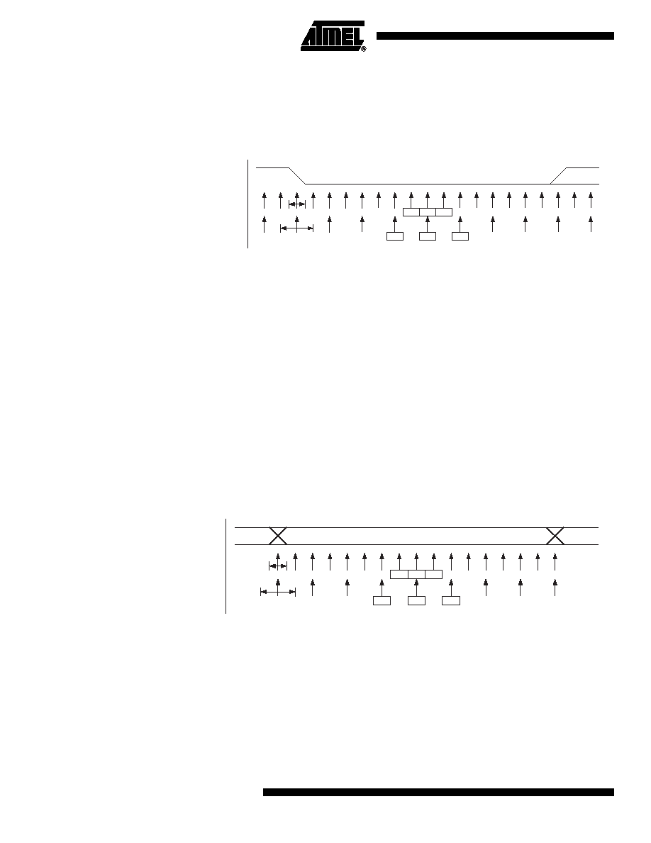
izontal arrows illustrate the synchronization variation due to the sampling process. Note the
larger time variation when using the Double Speed mode (U2Xn = 1) of operation. Samples
denoted zero are samples done when the RxDn line is idle (i.e., no communication activity).
Figure 17-5. Start Bit Sampling
When the clock recovery logic detects a high (idle) to low (start) transition on the RxDn line, the
start bit detection sequence is initiated. Let sample 1 denote the first zero-sample as shown in
the figure. The clock recovery logic then uses samples 8, 9, and 10 for Normal mode, and sam-
ples 4, 5, and 6 for Double Speed mode (indicated with sample numbers inside boxes on the
figure), to decide if a valid start bit is received. If two or more of these three samples have logical
high levels (the majority wins), the start bit is rejected as a noise spike and the Receiver starts
looking for the next high to low-transition. If however, a valid start bit is detected, the clock recov-
ery logic is synchronized and the data recovery can begin. The synchronization process is
repeated for each start bit.
17.9.2
Asynchronous Data Recovery
When the receiver clock is synchronized to the start bit, the data recovery can begin. The data
recovery unit uses a state machine that has 16 states for each bit in Normal mode and eight
states for each bit in Double Speed mode. Figure 17-6 shows the sampling of the data bits and
the parity bit. Each of the samples is given a number that is equal to the state of the recovery
unit.
Figure 17-6. Sampling of Data and Parity Bit
The decision of the logic level of the received bit is taken by doing a majority voting of the logic
value to the three samples in the center of the received bit. The center samples are emphasized
on the figure by having the sample number inside boxes. The majority voting process is done as
follows: If two or all three samples have high levels, the received bit is registered to be a logic 1.
If two or all three samples have low levels, the received bit is registered to be a logic 0. This
majority voting process acts as a low pass filter for the incoming signal on the RxDn pin. The
recovery process is then repeated until a complete frame is received. Including the first stop bit.
Note that the Receiver only uses the first stop bit of a frame.
1
2
3
4
5
6
7
8
9
10
11
12
13
14
15
16
1
2
START
IDLE
0
BIT
0
3
1
2
3
4
5
6
7
8
1
2
0
RxDn
Sample
(U2Xn
=
0)
Sample
(U2Xn
=
1)
1
2
3
4
5
6
7
8
9
10
11
12
13
14
15
16
1
BIT
x
1
2
3
4
5
6
7
8
1
RxDn
Sample
(U2Xn
=
0)
Sample
(U2Xn
=
1)
相关PDF资料 |
PDF描述 |
|---|---|
| VE-B4N-IW-F2 | CONVERTER MOD DC/DC 18.5V 100W |
| PIC12F752-I/MF | IC MCU 8BIT 1024B FLASH 8-DFN |
| PIC16F1503-I/P | MCU 8BIT 3.5KB FLASH 14PDIP |
| VE-B4N-IW-F1 | CONVERTER MOD DC/DC 18.5V 100W |
| VE-B4M-IX-F1 | CONVERTER MOD DC/DC 10V 75W |
相关代理商/技术参数 |
参数描述 |
|---|---|
| PIC12F752-I-SN | 制造商:MICROCHIP 制造商全称:Microchip Technology 功能描述:8-Pin, Flash-Based 8-Bit CMOS Microcontrollers |
| PIC12F752T-I/MF | 功能描述:8位微控制器 -MCU 1.75KB 64BRAM 6 I/O 8MHz Int Osc 5MIPS RoHS:否 制造商:Silicon Labs 核心:8051 处理器系列:C8051F39x 数据总线宽度:8 bit 最大时钟频率:50 MHz 程序存储器大小:16 KB 数据 RAM 大小:1 KB 片上 ADC:Yes 工作电源电压:1.8 V to 3.6 V 工作温度范围:- 40 C to + 105 C 封装 / 箱体:QFN-20 安装风格:SMD/SMT |
| PIC12F752T-I/SN | 功能描述:8位微控制器 -MCU 1.75KB 64BRAM 6 I/O 8MHz Int Osc 5MIPS RoHS:否 制造商:Silicon Labs 核心:8051 处理器系列:C8051F39x 数据总线宽度:8 bit 最大时钟频率:50 MHz 程序存储器大小:16 KB 数据 RAM 大小:1 KB 片上 ADC:Yes 工作电源电压:1.8 V to 3.6 V 工作温度范围:- 40 C to + 105 C 封装 / 箱体:QFN-20 安装风格:SMD/SMT |
| PIC12HV609-E/MD | 功能描述:8位微控制器 -MCU 1.75KB Flash, E TEMP 64B RAM, DFN8 RoHS:否 制造商:Silicon Labs 核心:8051 处理器系列:C8051F39x 数据总线宽度:8 bit 最大时钟频率:50 MHz 程序存储器大小:16 KB 数据 RAM 大小:1 KB 片上 ADC:Yes 工作电源电压:1.8 V to 3.6 V 工作温度范围:- 40 C to + 105 C 封装 / 箱体:QFN-20 安装风格:SMD/SMT |
| PIC12HV609-E/MF | 功能描述:8位微控制器 -MCU 1.75KB Flash 64B RAM 6 I/O 8MHz INT OSC RoHS:否 制造商:Silicon Labs 核心:8051 处理器系列:C8051F39x 数据总线宽度:8 bit 最大时钟频率:50 MHz 程序存储器大小:16 KB 数据 RAM 大小:1 KB 片上 ADC:Yes 工作电源电压:1.8 V to 3.6 V 工作温度范围:- 40 C to + 105 C 封装 / 箱体:QFN-20 安装风格:SMD/SMT |
发布紧急采购,3分钟左右您将得到回复。