- 您现在的位置:买卖IC网 > PDF目录11571 > PIC12LCE519T-04I/SM (Microchip Technology)IC MCU OTP 1KX12 LV W/EE 8-SOIJ PDF资料下载
参数资料
| 型号: | PIC12LCE519T-04I/SM |
| 厂商: | Microchip Technology |
| 文件页数: | 40/113页 |
| 文件大小: | 0K |
| 描述: | IC MCU OTP 1KX12 LV W/EE 8-SOIJ |
| 产品培训模块: | Asynchronous Stimulus |
| 标准包装: | 2,100 |
| 系列: | PIC® 12C |
| 核心处理器: | PIC |
| 芯体尺寸: | 8-位 |
| 速度: | 4MHz |
| 外围设备: | POR,WDT |
| 输入/输出数: | 5 |
| 程序存储器容量: | 1.5KB(1K x 12) |
| 程序存储器类型: | OTP |
| EEPROM 大小: | 16 x 8 |
| RAM 容量: | 41 x 8 |
| 电压 - 电源 (Vcc/Vdd): | 2.5 V ~ 5.5 V |
| 振荡器型: | 内部 |
| 工作温度: | -40°C ~ 85°C |
| 封装/外壳: | 8-SOIC(0.209",5.30mm 宽) |
| 包装: | 带卷 (TR) |
| 其它名称: | PIC12LCE519T04ISM |
第1页第2页第3页第4页第5页第6页第7页第8页第9页第10页第11页第12页第13页第14页第15页第16页第17页第18页第19页第20页第21页第22页第23页第24页第25页第26页第27页第28页第29页第30页第31页第32页第33页第34页第35页第36页第37页第38页第39页当前第40页第41页第42页第43页第44页第45页第46页第47页第48页第49页第50页第51页第52页第53页第54页第55页第56页第57页第58页第59页第60页第61页第62页第63页第64页第65页第66页第67页第68页第69页第70页第71页第72页第73页第74页第75页第76页第77页第78页第79页第80页第81页第82页第83页第84页第85页第86页第87页第88页第89页第90页第91页第92页第93页第94页第95页第96页第97页第98页第99页第100页第101页第102页第103页第104页第105页第106页第107页第108页第109页第110页第111页第112页第113页
PIC12C5XX
DS40139E-page 32
1999 Microchip Technology Inc.
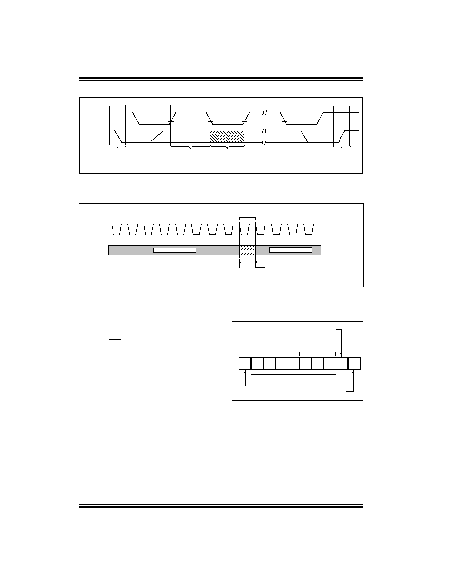
FIGURE 7-3:
DATA TRANSFER SEQUENCE ON THE SERIAL BUS
FIGURE 7-4:
ACKNOWLEDGE TIMING
(A)
(B)
(C)
(D)
(A)
(C)
SCL
SDA
START
CONDITION
ADDRESS OR
ACKNOWLEDGE
VALID
DATA
ALLOWED
TO CHANGE
STOP
CONDITION
SCL
9
8
7
6
5
4
3
2
11
2
3
Transmitter must release the SDA line at this point
allowing the Receiver to pull the SDA line low to
acknowledge the previous eight bits of data.
Receiver must release the SDA line at this point
so the Transmitter can continue sending data.
Data from transmitter
SDA
Acknowledge
Bit
7.2
Device Addressing
After generating a START condition, the bus master
transmits a control byte consisting of a slave address
and a Read/Write bit that indicates what type of opera-
tion is to be performed. The slave address consists of
a 4-bit device code (1010) followed by three don’t care
bits.
The last bit of the control byte determines the operation
to be performed. When set to a one a read operation is
selected, and when set to a zero a write operation is
selected. (Figure 7-5). The bus is monitored for its cor-
responding slave address all the time. It generates an
acknowledge bit if the slave address was true and it is
not in a programming mode.
FIGURE 7-5:
CONTROL BYTE FORMAT
10
1
0
X
SACK
R/W
Device Select
Bits
Don’t Care
Bits
Slave Address
Acknowledge Bit
Start Bit
Read/Write Bit
相关PDF资料 |
PDF描述 |
|---|---|
| V300A28C400BF | CONVERTER MOD DC/DC 28V 400W |
| PIC18LF13K50T-I/SS | IC PIC MCU FLASH 8KB 20-SSOP |
| PIC16LF1782-E/MV | IC MCU 8BIT 3.5KB FLASH 28-UQFN |
| VE-21J-IX-S | CONVERTER MOD DC/DC 36V 75W |
| VI-21J-IX-S | CONVERTER MOD DC/DC 36V 75W |
相关代理商/技术参数 |
参数描述 |
|---|---|
| PIC12LCE673-04/P | 功能描述:8位微控制器 -MCU 1.75KB 128 RAM 6 I/O RoHS:否 制造商:Silicon Labs 核心:8051 处理器系列:C8051F39x 数据总线宽度:8 bit 最大时钟频率:50 MHz 程序存储器大小:16 KB 数据 RAM 大小:1 KB 片上 ADC:Yes 工作电源电压:1.8 V to 3.6 V 工作温度范围:- 40 C to + 105 C 封装 / 箱体:QFN-20 安装风格:SMD/SMT |
| PIC12LCE673-04I/P | 功能描述:8位微控制器 -MCU 1.75KB 128 RAM 6 I/O RoHS:否 制造商:Silicon Labs 核心:8051 处理器系列:C8051F39x 数据总线宽度:8 bit 最大时钟频率:50 MHz 程序存储器大小:16 KB 数据 RAM 大小:1 KB 片上 ADC:Yes 工作电源电压:1.8 V to 3.6 V 工作温度范围:- 40 C to + 105 C 封装 / 箱体:QFN-20 安装风格:SMD/SMT |
| PIC12LCE674-04/P | 功能描述:8位微控制器 -MCU 3.5KB 128 RAM 6 I/O RoHS:否 制造商:Silicon Labs 核心:8051 处理器系列:C8051F39x 数据总线宽度:8 bit 最大时钟频率:50 MHz 程序存储器大小:16 KB 数据 RAM 大小:1 KB 片上 ADC:Yes 工作电源电压:1.8 V to 3.6 V 工作温度范围:- 40 C to + 105 C 封装 / 箱体:QFN-20 安装风格:SMD/SMT |
| PIC12LCE674-04I/P | 功能描述:8位微控制器 -MCU 3.5KB 128 RAM 6 I/O RoHS:否 制造商:Silicon Labs 核心:8051 处理器系列:C8051F39x 数据总线宽度:8 bit 最大时钟频率:50 MHz 程序存储器大小:16 KB 数据 RAM 大小:1 KB 片上 ADC:Yes 工作电源电压:1.8 V to 3.6 V 工作温度范围:- 40 C to + 105 C 封装 / 箱体:QFN-20 安装风格:SMD/SMT |
| PIC12LF1501-E/MC | 功能描述:8位微控制器 -MCU 1.75KB Fl 64B RAM 6 I/O 10-bit ADC RoHS:否 制造商:Silicon Labs 核心:8051 处理器系列:C8051F39x 数据总线宽度:8 bit 最大时钟频率:50 MHz 程序存储器大小:16 KB 数据 RAM 大小:1 KB 片上 ADC:Yes 工作电源电压:1.8 V to 3.6 V 工作温度范围:- 40 C to + 105 C 封装 / 箱体:QFN-20 安装风格:SMD/SMT |
发布紧急采购,3分钟左右您将得到回复。