- 您现在的位置:买卖IC网 > PDF目录11758 > PIC16C433-I/P (Microchip Technology)IC MCU CMOS 8BIT 10MHZ 2K 18-DIP PDF资料下载
参数资料
| 型号: | PIC16C433-I/P |
| 厂商: | Microchip Technology |
| 文件页数: | 10/126页 |
| 文件大小: | 0K |
| 描述: | IC MCU CMOS 8BIT 10MHZ 2K 18-DIP |
| 产品培训模块: | Asynchronous Stimulus 8-bit PIC® Microcontroller Portfolio |
| 标准包装: | 25 |
| 系列: | PIC® 16C |
| 核心处理器: | PIC |
| 芯体尺寸: | 8-位 |
| 速度: | 10MHz |
| 连通性: | LIN(本地互连网络) |
| 外围设备: | POR,WDT |
| 输入/输出数: | 5 |
| 程序存储器容量: | 3.5KB(2K x 14) |
| 程序存储器类型: | OTP |
| RAM 容量: | 128 x 8 |
| 电压 - 电源 (Vcc/Vdd): | 4.5 V ~ 5.5 V |
| 数据转换器: | A/D 4x8b |
| 振荡器型: | 内部 |
| 工作温度: | -40°C ~ 85°C |
| 封装/外壳: | 18-DIP(0.300",7.62mm) |
| 包装: | 管件 |
| 产品目录页面: | 636 (CN2011-ZH PDF) |
| 配用: | DVA16XP185-ND - ADAPTER DEVICE ICE 18DIP/SOIC |
第1页第2页第3页第4页第5页第6页第7页第8页第9页当前第10页第11页第12页第13页第14页第15页第16页第17页第18页第19页第20页第21页第22页第23页第24页第25页第26页第27页第28页第29页第30页第31页第32页第33页第34页第35页第36页第37页第38页第39页第40页第41页第42页第43页第44页第45页第46页第47页第48页第49页第50页第51页第52页第53页第54页第55页第56页第57页第58页第59页第60页第61页第62页第63页第64页第65页第66页第67页第68页第69页第70页第71页第72页第73页第74页第75页第76页第77页第78页第79页第80页第81页第82页第83页第84页第85页第86页第87页第88页第89页第90页第91页第92页第93页第94页第95页第96页第97页第98页第99页第100页第101页第102页第103页第104页第105页第106页第107页第108页第109页第110页第111页第112页第113页第114页第115页第116页第117页第118页第119页第120页第121页第122页第123页第124页第125页第126页
107
4378C–AVR–09/08
AT90PWM1
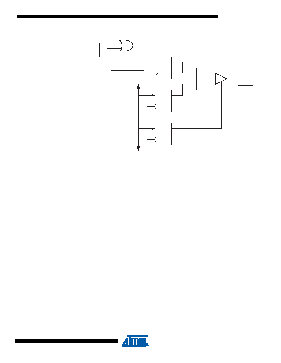
Figure 15-5. Compare Match Output Unit, Schematic
The general I/O port function is overridden by the Output Compare (OCnx) from the Waveform
Generator if either of the COMnx1:0 bits are set. However, the OCnx pin direction (input or out-
put) is still controlled by the Data Direction Register (DDR) for the port pin. The Data Direction
Register bit for the OCnx pin (DDR_OCnx) must be set as output before the OCnx value is visi-
ble on the pin. The port override function is generally independent of the Waveform Generation
The design of the Output Compare pin logic allows initialization of the OCnx state before the out-
put is enabled. Note that some COMnx1:0 bit settings are reserved for certain modes of
The COMnx1:0 bits have no effect on the Input Capture unit.
15.7.1
Compare Output Mode and Waveform Generation
The Waveform Generator uses the COMnx1:0 bits differently in normal, CTC, and PWM modes.
For all modes, setting the COMnx1:0 = 0 tells the Waveform Generator that no action on the
OCnx Register is to be performed on the next compare match. For compare output actions in the
non-PWM modes refer to Table 29 on page 117. For fast PWM mode refer to Table 30 on page
117, and for phase correct and phase and frequency correct PWM refer to Table 31 on page
A change of the COMnx1:0 bits state will have effect at the first compare match after the bits are
written. For non-PWM modes, the action can be forced to have immediate effect by using the
FOCnx strobe bits.
15.8
Modes of Operation
The mode of operation, i.e., the behavior of the Timer/Counter and the Output Compare pins, is
defined by the combination of the Waveform Generation mode (WGMn3:0) and Compare Output
mode (COMnx1:0) bits. The Compare Output mode bits do not affect the counting sequence,
while the Waveform Generation mode bits do. The COMnx1:0 bits control whether the PWM out-
PORT
DDR
DQ
OCnx
Pin
OCnx
DQ
Waveform
Generator
COMnx1
COMnx0
0
1
D
ATA
B
U
S
FOCnx
clk
I/O
相关PDF资料 |
PDF描述 |
|---|---|
| D38999/26FC4PN | CONN PLUG 4POS STRAIGHT W/PINS |
| 5413959-6 | CONN PLUG BNC RG141 R/A CRIMP AU |
| PIC18LF24J11-I/SS | IC PIC MCU FLASH 16K 2V 28-SSOP |
| D38999/26WC4PN | CONN PLUG 4POS STRAIGHT W/PINS |
| 5225392-7 | CONN PLUG N-TYPE RG-58 CRIMP |
相关代理商/技术参数 |
参数描述 |
|---|---|
| PIC16C433T-E/SO | 功能描述:8位微控制器 -MCU 3.5KB 128 RAM 6 I/O RoHS:否 制造商:Silicon Labs 核心:8051 处理器系列:C8051F39x 数据总线宽度:8 bit 最大时钟频率:50 MHz 程序存储器大小:16 KB 数据 RAM 大小:1 KB 片上 ADC:Yes 工作电源电压:1.8 V to 3.6 V 工作温度范围:- 40 C to + 105 C 封装 / 箱体:QFN-20 安装风格:SMD/SMT |
| PIC16C433T-I/SO | 功能描述:8位微控制器 -MCU 3.5KB 128 RAM 6 I/O RoHS:否 制造商:Silicon Labs 核心:8051 处理器系列:C8051F39x 数据总线宽度:8 bit 最大时钟频率:50 MHz 程序存储器大小:16 KB 数据 RAM 大小:1 KB 片上 ADC:Yes 工作电源电压:1.8 V to 3.6 V 工作温度范围:- 40 C to + 105 C 封装 / 箱体:QFN-20 安装风格:SMD/SMT |
| PIC16C505/JW | 功能描述:8位微控制器 -MCU 1.5KB 72 RAM 12 I/O RoHS:否 制造商:Silicon Labs 核心:8051 处理器系列:C8051F39x 数据总线宽度:8 bit 最大时钟频率:50 MHz 程序存储器大小:16 KB 数据 RAM 大小:1 KB 片上 ADC:Yes 工作电源电压:1.8 V to 3.6 V 工作温度范围:- 40 C to + 105 C 封装 / 箱体:QFN-20 安装风格:SMD/SMT |
| PIC16C505-04/P | 功能描述:8位微控制器 -MCU 1.5KB 72 RAM 12 I/O 4MHz PDIP14 RoHS:否 制造商:Silicon Labs 核心:8051 处理器系列:C8051F39x 数据总线宽度:8 bit 最大时钟频率:50 MHz 程序存储器大小:16 KB 数据 RAM 大小:1 KB 片上 ADC:Yes 工作电源电压:1.8 V to 3.6 V 工作温度范围:- 40 C to + 105 C 封装 / 箱体:QFN-20 安装风格:SMD/SMT |
| PIC16C505-04/P | 制造商:Microchip Technology Inc 功能描述:IC 8BIT CMOS MCU (TUBE 30) 16C505 制造商:Microchip Technology Inc 功能描述:IC 8BIT CMOS MCU 16C505 DIP14 |
发布紧急采购,3分钟左右您将得到回复。