- 您现在的位置:买卖IC网 > PDF目录11767 > PIC16C505-04I/P (Microchip Technology)IC MCU OTP 1KX12 14DIP PDF资料下载
参数资料
| 型号: | PIC16C505-04I/P |
| 厂商: | Microchip Technology |
| 文件页数: | 16/90页 |
| 文件大小: | 0K |
| 描述: | IC MCU OTP 1KX12 14DIP |
| 产品培训模块: | Asynchronous Stimulus 8-bit PIC® Microcontroller Portfolio |
| 标准包装: | 30 |
| 系列: | PIC® 16C |
| 核心处理器: | PIC |
| 芯体尺寸: | 8-位 |
| 速度: | 4MHz |
| 外围设备: | POR,WDT |
| 输入/输出数: | 11 |
| 程序存储器容量: | 1.5KB(1K x 12) |
| 程序存储器类型: | OTP |
| RAM 容量: | 72 x 8 |
| 电压 - 电源 (Vcc/Vdd): | 3 V ~ 5.5 V |
| 振荡器型: | 内部 |
| 工作温度: | -40°C ~ 85°C |
| 封装/外壳: | 14-DIP(0.300",7.62mm) |
| 包装: | 管件 |
| 配用: | ISPICR1-ND - ADAPTER IN-CIRCUIT PROGRAMMING 309-1086-ND - ADAPTER 14-ZIF BD W/14-SO PLUGS 309-1085-ND - ADAPTER 14-DIP BD W/2 14-SO PLUG AC124001-ND - MODULE SKT PROMATEII 8DIP/SOIC |
第1页第2页第3页第4页第5页第6页第7页第8页第9页第10页第11页第12页第13页第14页第15页当前第16页第17页第18页第19页第20页第21页第22页第23页第24页第25页第26页第27页第28页第29页第30页第31页第32页第33页第34页第35页第36页第37页第38页第39页第40页第41页第42页第43页第44页第45页第46页第47页第48页第49页第50页第51页第52页第53页第54页第55页第56页第57页第58页第59页第60页第61页第62页第63页第64页第65页第66页第67页第68页第69页第70页第71页第72页第73页第74页第75页第76页第77页第78页第79页第80页第81页第82页第83页第84页第85页第86页第87页第88页第89页第90页
1999-2012 Microchip Technology Inc.
DS40192D-page 23
PIC16C505
6.0
TIMER0 MODULE AND TMR0
REGISTER
The Timer0 module has the following features:
8-bit timer/counter register, TMR0
- Readable and writable
8-bit software programmable prescaler
Internal or external clock select
- Edge select for external clock
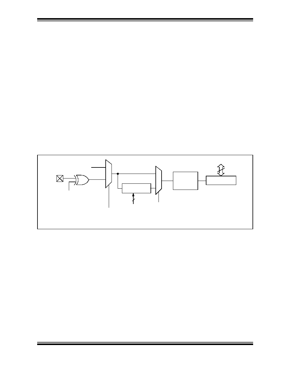
Figure 6-1 is a simplified block diagram of the Timer0
module.
Timer mode is selected by clearing the T0CS bit
(OPTION<5>). In timer mode, the Timer0 module will
increment every instruction cycle (without prescaler). If
TMR0 register is written, the increment is inhibited for
the following two cycles (Figure 6-2 and Figure 6-3).
The user can work around this by writing an adjusted
value to the TMR0 register.
Counter mode is selected by setting the T0CS bit
(OPTION<5>). In this mode, Timer0 will increment
either on every rising or falling edge of pin T0CKI. The
T0SE bit (OPTION<4>) determines the source edge.
Clearing the T0SE bit selects the rising edge.
Restrictions on the external clock input are discussed
in detail in Section 6.1.
The prescaler may be used by either the Timer0
module or the Watchdog Timer, but not both. The
prescaler assignment is controlled in software by the
control bit PSA (OPTION<3>). Clearing the PSA bit
will assign the prescaler to Timer0. The prescaler is
not readable or writable. When the prescaler is
assigned to the Timer0 module, prescale values of 1:2,
1:4,..., 1:256 are selectable. Section 6.2 details the
operation of the prescaler.
A summary of registers associated with the Timer0
module is found in Table 6-1.
FIGURE 6-1:
TIMER0 BLOCK DIAGRAM
Note 1: Bits T0CS, T0SE, PSA, PS2, PS1 and PS0 are located in the OPTION register.
2: The prescaler is shared with the Watchdog Timer (Figure 6-5).
0
1
0
T0CS(1)
FOSC/4
Programmable
Prescaler(2)
Sync with
Internal
Clocks
TMR0 reg
PSout
(2 TCY delay)
PSout
Data Bus
8
PSA(1)
PS2, PS1, PS0(1)
3
Sync
T0SE
RC5/T0CKI
Pin
相关PDF资料 |
PDF描述 |
|---|---|
| VI-B44-IW-F3 | CONVERTER MOD DC/DC 48V 100W |
| VI-B42-IW-F4 | CONVERTER MOD DC/DC 15V 100W |
| VI-B44-IW-F2 | CONVERTER MOD DC/DC 48V 100W |
| PIC16F1825-E/SL | MCU PIC 14K FLASH 1K RAM 14SOIC |
| VI-B43-IX-F4 | CONVERTER MOD DC/DC 24V 75W |
相关代理商/技术参数 |
参数描述 |
|---|---|
| PIC16C505-20/P | 功能描述:8位微控制器 -MCU 1.5KB 72 RAM 12 I/O 20MHz PDIP14 RoHS:否 制造商:Silicon Labs 核心:8051 处理器系列:C8051F39x 数据总线宽度:8 bit 最大时钟频率:50 MHz 程序存储器大小:16 KB 数据 RAM 大小:1 KB 片上 ADC:Yes 工作电源电压:1.8 V to 3.6 V 工作温度范围:- 40 C to + 105 C 封装 / 箱体:QFN-20 安装风格:SMD/SMT |
| PIC16C505-20/SL | 功能描述:8位微控制器 -MCU 1.5KB 72 RAM 12 I/O 20MHz SOIC14 RoHS:否 制造商:Silicon Labs 核心:8051 处理器系列:C8051F39x 数据总线宽度:8 bit 最大时钟频率:50 MHz 程序存储器大小:16 KB 数据 RAM 大小:1 KB 片上 ADC:Yes 工作电源电压:1.8 V to 3.6 V 工作温度范围:- 40 C to + 105 C 封装 / 箱体:QFN-20 安装风格:SMD/SMT |
| PIC16C505-20E/P | 功能描述:8位微控制器 -MCU 1.5KB 72 RAM 12 I/O 20MHz ExtTemp PDIP14 RoHS:否 制造商:Silicon Labs 核心:8051 处理器系列:C8051F39x 数据总线宽度:8 bit 最大时钟频率:50 MHz 程序存储器大小:16 KB 数据 RAM 大小:1 KB 片上 ADC:Yes 工作电源电压:1.8 V to 3.6 V 工作温度范围:- 40 C to + 105 C 封装 / 箱体:QFN-20 安装风格:SMD/SMT |
| PIC16C505-20E/SL | 功能描述:8位微控制器 -MCU 1.5KB 72 RAM 12 I/O 20MHz ExtTemp SOIC14 RoHS:否 制造商:Silicon Labs 核心:8051 处理器系列:C8051F39x 数据总线宽度:8 bit 最大时钟频率:50 MHz 程序存储器大小:16 KB 数据 RAM 大小:1 KB 片上 ADC:Yes 工作电源电压:1.8 V to 3.6 V 工作温度范围:- 40 C to + 105 C 封装 / 箱体:QFN-20 安装风格:SMD/SMT |
| PIC16C505-20I/P | 功能描述:8位微控制器 -MCU 1.5KB 72 RAM 12 I/O 20MHz IndTemp PDIP14 RoHS:否 制造商:Silicon Labs 核心:8051 处理器系列:C8051F39x 数据总线宽度:8 bit 最大时钟频率:50 MHz 程序存储器大小:16 KB 数据 RAM 大小:1 KB 片上 ADC:Yes 工作电源电压:1.8 V to 3.6 V 工作温度范围:- 40 C to + 105 C 封装 / 箱体:QFN-20 安装风格:SMD/SMT |
发布紧急采购,3分钟左右您将得到回复。