- 您现在的位置:买卖IC网 > PDF目录11560 > PIC16C54C-20E/SO (Microchip Technology)IC MCU OTP 512X12 18SOIC PDF资料下载
参数资料
| 型号: | PIC16C54C-20E/SO |
| 厂商: | Microchip Technology |
| 文件页数: | 15/194页 |
| 文件大小: | 0K |
| 描述: | IC MCU OTP 512X12 18SOIC |
| 产品培训模块: | Asynchronous Stimulus |
| 标准包装: | 42 |
| 系列: | PIC® 16C |
| 核心处理器: | PIC |
| 芯体尺寸: | 8-位 |
| 速度: | 20MHz |
| 外围设备: | POR,WDT |
| 输入/输出数: | 12 |
| 程序存储器容量: | 768B(512 x 12) |
| 程序存储器类型: | OTP |
| RAM 容量: | 25 x 8 |
| 电压 - 电源 (Vcc/Vdd): | 3 V ~ 5.5 V |
| 振荡器型: | 外部 |
| 工作温度: | -40°C ~ 125°C |
| 封装/外壳: | 18-SOIC(0.295",7.50mm 宽) |
| 包装: | 管件 |
第1页第2页第3页第4页第5页第6页第7页第8页第9页第10页第11页第12页第13页第14页当前第15页第16页第17页第18页第19页第20页第21页第22页第23页第24页第25页第26页第27页第28页第29页第30页第31页第32页第33页第34页第35页第36页第37页第38页第39页第40页第41页第42页第43页第44页第45页第46页第47页第48页第49页第50页第51页第52页第53页第54页第55页第56页第57页第58页第59页第60页第61页第62页第63页第64页第65页第66页第67页第68页第69页第70页第71页第72页第73页第74页第75页第76页第77页第78页第79页第80页第81页第82页第83页第84页第85页第86页第87页第88页第89页第90页第91页第92页第93页第94页第95页第96页第97页第98页第99页第100页第101页第102页第103页第104页第105页第106页第107页第108页第109页第110页第111页第112页第113页第114页第115页第116页第117页第118页第119页第120页第121页第122页第123页第124页第125页第126页第127页第128页第129页第130页第131页第132页第133页第134页第135页第136页第137页第138页第139页第140页第141页第142页第143页第144页第145页第146页第147页第148页第149页第150页第151页第152页第153页第154页第155页第156页第157页第158页第159页第160页第161页第162页第163页第164页第165页第166页第167页第168页第169页第170页第171页第172页第173页第174页第175页第176页第177页第178页第179页第180页第181页第182页第183页第184页第185页第186页第187页第188页第189页第190页第191页第192页第193页第194页
PIC18F2450/4450
2006 Microchip Technology Inc.
Advance Information
DS39760A-page 109
9.5
PORTE, TRISE and LATE
Registers
Depending on the particular PIC18F2450/4450 device
selected, PORTE is implemented in two different ways.
For 40/44-pin devices, PORTE is a 4-bit wide port.
Three pins (RE0/AN5, RE1/AN6 and RE2/AN7) are
individually configurable as inputs or outputs. These
pins have Schmitt Trigger input buffers. When selected
as an analog input, these pins will read as ‘0’s.
The corresponding data direction register is TRISE.
Setting a TRISE bit (= 1) will make the corresponding
PORTE pin an input (i.e., put the corresponding output
driver in a high-impedance mode). Clearing a TRISE bit
(= 0) will make the corresponding PORTE pin an output
(i.e., put the contents of the output latch on the selected
pin).
TRISE controls the direction of the RE pins, even when
they are being used as analog inputs. The user must
make sure to keep the pins configured as inputs when
using them as analog inputs.
The Data Latch register (LATE) is also memory
mapped. Read-modify-write operations on the LATE
register read and write the latched output value for
PORTE.
The fourth pin of PORTE (MCLR/VPP/RE3) is an input
only pin. Its operation is controlled by the MCLRE Config-
uration bit. When selected as a port pin (MCLRE = 0), it
functions as a digital input only pin; as such, it does not
have TRIS or LAT bits associated with its operation.
Otherwise, it functions as the device’s Master Clear input.
In either configuration, RE3 also functions as the
programming voltage input during programming.
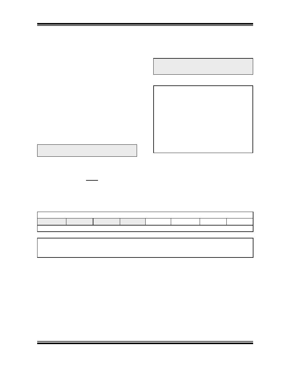
EXAMPLE 9-5:
INITIALIZING PORTE
9.5.1
PORTE IN 28-PIN DEVICES
For 28-pin devices, PORTE is only available when
Master Clear functionality is disabled (MCLRE = 0). In
these cases, PORTE is a single bit, input only port
comprised of RE3 only. The pin operates as previously
described.
Note:
On a Power-on Reset, RE2:RE0 are
configured as analog inputs.
Note:
On a Power-on Reset, RE3 is enabled as
a digital input only if Master Clear
functionality is disabled.
CLRF
PORTE
; Initialize PORTE by
; clearing output
; data latches
CLRF
LATE
; Alternate method
; to clear output
; data latches
MOVLW
0Ah
; Configure A/D
MOVWF
ADCON1
; for digital inputs
MOVLW
03h
; Value used to
; initialize data
; direction
MOVWF
TRISC
; Set RE<0> as inputs
; RE<1> as inputs
; RE<2> as outputs
REGISTER 9-1:
PORTE REGISTER
U-0
R/W-x
R/W-0
—
RE3(1,2)
RE2(3)
RE1(3)
RE0(3)
bit 7
bit 0
Legend:
R = Readable bit
W = Writable bit
U = Unimplemented bit, read as ‘0’
-n = Value at POR
‘1’ = Bit is set
‘0’ = Bit is cleared
x = Bit is unknown
bit 7-4
Unimplemented: Read as ‘0’
bit 3-0
RE3:RE0: PORTE Data Input bits(1,2,3)
Note 1:
implemented only when Master Clear functionality is disabled (MCLRE Configuration bit = 0); otherwise,
read as ‘0’.
2:
RE3 is the only PORTE bit implemented on both 28-pin and 40/44-pin devices. All other bits are
implemented only when PORTE is implemented (i.e., 40/44-pin devices).
3:
Unimplemented in 28-pin devices; read as ‘0’.
相关PDF资料 |
PDF描述 |
|---|---|
| PIC16C54C-04E/SS | IC MCU OTP 512X12 20SSOP |
| PIC12C509T-04/SM | IC MCU OTP 1KX12 8-SOIJ |
| PIC12C508T-04I/SM | IC MCU OTP 512X12 8-SOIJ |
| PIC24F16KL402T-I/SO | IC MCU 16BIT 16KB FLASH 28-SOIC |
| PIC16LF627A-I/ML | IC MCU FLASH 1KX14 EEPROM 28QFN |
相关代理商/技术参数 |
参数描述 |
|---|---|
| PIC16C54C-20I/P | 功能描述:8位微控制器 -MCU .75KB 25 RAM 12 I/O 20MHz IndTemp PDIP18 RoHS:否 制造商:Silicon Labs 核心:8051 处理器系列:C8051F39x 数据总线宽度:8 bit 最大时钟频率:50 MHz 程序存储器大小:16 KB 数据 RAM 大小:1 KB 片上 ADC:Yes 工作电源电压:1.8 V to 3.6 V 工作温度范围:- 40 C to + 105 C 封装 / 箱体:QFN-20 安装风格:SMD/SMT |
| PIC16C54C-20I/P | 制造商:Microchip Technology Inc 功能描述:IC 8BIT CMOS MCU 16C54 DIP18 |
| PIC16C54C-20I/SO | 功能描述:8位微控制器 -MCU .75KB 25 RAM 12 I/O 20MHz IndTemp SOIC18 RoHS:否 制造商:Silicon Labs 核心:8051 处理器系列:C8051F39x 数据总线宽度:8 bit 最大时钟频率:50 MHz 程序存储器大小:16 KB 数据 RAM 大小:1 KB 片上 ADC:Yes 工作电源电压:1.8 V to 3.6 V 工作温度范围:- 40 C to + 105 C 封装 / 箱体:QFN-20 安装风格:SMD/SMT |
| PIC16C54C-20I/SO | 制造商:Microchip Technology Inc 功能描述:8BIT CMOS MCU SMD 16C54 SOIC18 |
| PIC16C54C-20I/SS | 功能描述:8位微控制器 -MCU .75KB 25 RAM 12 I/O 20MHz IndTemp SSOP20 RoHS:否 制造商:Silicon Labs 核心:8051 处理器系列:C8051F39x 数据总线宽度:8 bit 最大时钟频率:50 MHz 程序存储器大小:16 KB 数据 RAM 大小:1 KB 片上 ADC:Yes 工作电源电压:1.8 V to 3.6 V 工作温度范围:- 40 C to + 105 C 封装 / 箱体:QFN-20 安装风格:SMD/SMT |
发布紧急采购,3分钟左右您将得到回复。