参数资料
| 型号: | PIC16C55-XT/SO |
| 厂商: | Microchip Technology |
| 文件页数: | 21/194页 |
| 文件大小: | 0K |
| 描述: | IC MCU OTP 512X12 28SOIC |
| 产品培训模块: | Asynchronous Stimulus 8-bit PIC® Microcontroller Portfolio |
| 标准包装: | 27 |
| 系列: | PIC® 16C |
| 核心处理器: | PIC |
| 芯体尺寸: | 8-位 |
| 速度: | 4MHz |
| 外围设备: | POR,WDT |
| 输入/输出数: | 20 |
| 程序存储器容量: | 768B(512 x 12) |
| 程序存储器类型: | OTP |
| RAM 容量: | 24 x 8 |
| 电压 - 电源 (Vcc/Vdd): | 3 V ~ 6.25 V |
| 振荡器型: | 外部 |
| 工作温度: | 0°C ~ 70°C |
| 封装/外壳: | 28-SOIC(0.295",7.50mm 宽) |
| 包装: | 管件 |
| 配用: | XLT28SO-1-ND - SOCKET TRANSITION 28SOIC 300MIL 309-1073-ND - ADAPTER 28-SOIC TO 28-SOIC 309-1024-ND - ADAPTER 28-SOIC TO 28-DIP 309-1023-ND - ADAPTER 28-SOIC TO 28-DIP 309-1011-ND - ADAPTER 18-SOIC TO 18-DIP 309-1010-ND - ADAPTER 18-SOIC TO 18-DIP AC164002-ND - MODULE SKT PROMATEII 18/28SOIC |
第1页第2页第3页第4页第5页第6页第7页第8页第9页第10页第11页第12页第13页第14页第15页第16页第17页第18页第19页第20页当前第21页第22页第23页第24页第25页第26页第27页第28页第29页第30页第31页第32页第33页第34页第35页第36页第37页第38页第39页第40页第41页第42页第43页第44页第45页第46页第47页第48页第49页第50页第51页第52页第53页第54页第55页第56页第57页第58页第59页第60页第61页第62页第63页第64页第65页第66页第67页第68页第69页第70页第71页第72页第73页第74页第75页第76页第77页第78页第79页第80页第81页第82页第83页第84页第85页第86页第87页第88页第89页第90页第91页第92页第93页第94页第95页第96页第97页第98页第99页第100页第101页第102页第103页第104页第105页第106页第107页第108页第109页第110页第111页第112页第113页第114页第115页第116页第117页第118页第119页第120页第121页第122页第123页第124页第125页第126页第127页第128页第129页第130页第131页第132页第133页第134页第135页第136页第137页第138页第139页第140页第141页第142页第143页第144页第145页第146页第147页第148页第149页第150页第151页第152页第153页第154页第155页第156页第157页第158页第159页第160页第161页第162页第163页第164页第165页第166页第167页第168页第169页第170页第171页第172页第173页第174页第175页第176页第177页第178页第179页第180页第181页第182页第183页第184页第185页第186页第187页第188页第189页第190页第191页第192页第193页第194页
PIC18F2450/4450
2006 Microchip Technology Inc.
Advance Information
DS39760A-page 115
11.0
TIMER1 MODULE
The Timer1 timer/counter module incorporates these
features:
Software selectable operation as a 16-bit timer or
counter
Readable and writable 8-bit registers (TMR1H
and TMR1L)
Selectable clock source (internal or external) with
device clock or Timer1 oscillator internal options
Interrupt on overflow
Module Reset on CCP Special Event Trigger
Device clock status flag (T1RUN)
A simplified block diagram of the Timer1 module is
shown in Figure 11-1. A block diagram of the module’s
operation in Read/Write mode is shown in Figure 11-2.
The module incorporates its own low-power oscillator
to provide an additional clocking option. The Timer1
oscillator can also be used as a low-power clock source
for the microcontroller in power-managed operation.
Timer1 can also be used to provide Real-Time Clock
(RTC) functionality to applications with only a minimal
addition of external components and code overhead.
Timer1 is controlled through the T1CON Control
register (Register 11-1). It also contains the Timer1
Oscillator Enable bit (T1OSCEN). Timer1 can be
enabled or disabled by setting or clearing control bit,
TMR1ON (T1CON<0>).
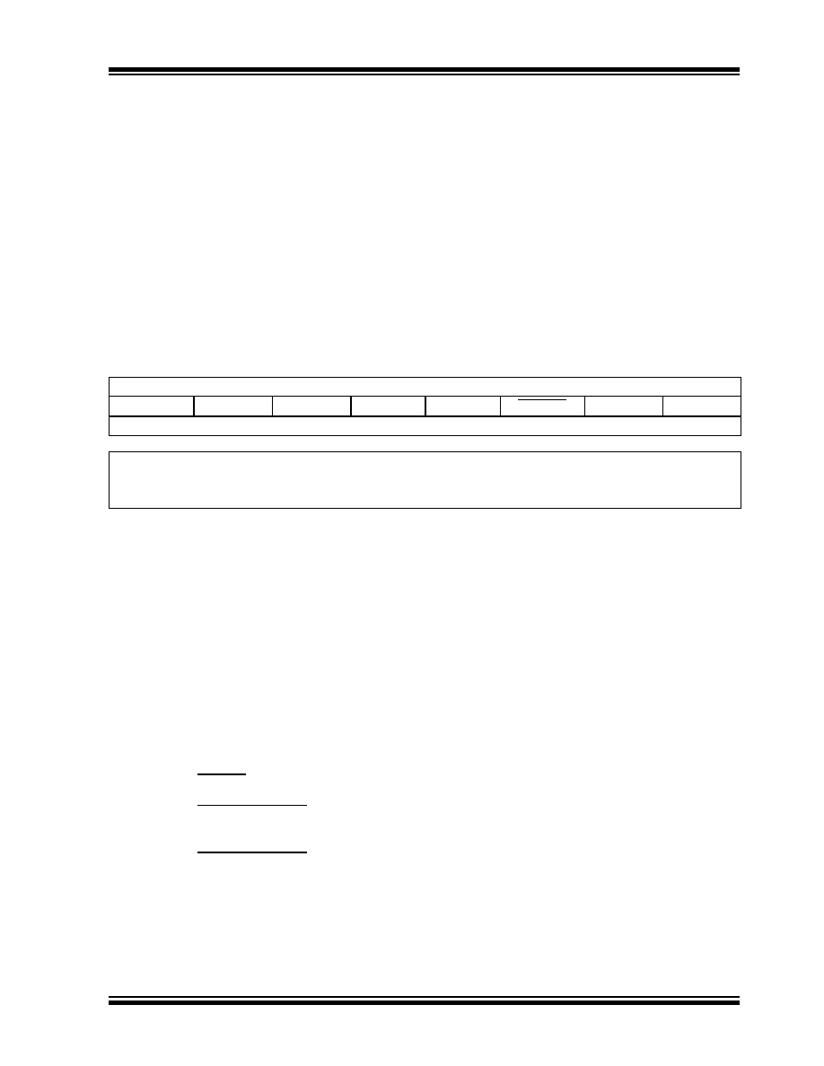
REGISTER 11-1:
T1CON: TIMER1 CONTROL REGISTER
R/W-0
R-0
R/W-0
RD16
T1RUN
T1CKPS1
T1CKPS0
T1OSCEN
T1SYNC
TMR1CS
TMR1ON
bit 7
bit 0
Legend:
R = Readable bit
W = Writable bit
U = Unimplemented bit, read as ‘0’
-n = Value at POR
‘1’ = Bit is set
‘0’ = Bit is cleared
x = Bit is unknown
bit 7
RD16: 16-Bit Read/Write Mode Enable bit
1
= Enables register read/write of Timer1 in one 16-bit operation
0
= Enables register read/write of Timer1 in two 8-bit operations
bit 6
T1RUN: Timer1 System Clock Status bit
1
= Device clock is derived from Timer1 oscillator
0
= Device clock is derived from another source
bit 5-4
T1CKPS1:T1CKPS0: Timer1 Input Clock Prescale Select bits
11
= 1:8 Prescale value
10
= 1:4 Prescale value
01
= 1:2 Prescale value
00
= 1:1 Prescale value
bit 3
T1OSCEN: Timer1 Oscillator Enable bit
1
= Timer1 oscillator is enabled
0
= Timer1 oscillator is shut off
The oscillator inverter and feedback resistor are turned off to eliminate power drain.
bit 2
T1SYNC: Timer1 External Clock Input Synchronization Select bit
When TMR1CS = 1:
1
= Do not synchronize external clock input
0
= Synchronize external clock input
When TMR1CS = 0:
This bit is ignored. Timer1 uses the internal clock when TMR1CS = 0.
bit 1
TMR1CS: Timer1 Clock Source Select bit
1
= External clock from RC0/T1OSO/T1CKI pin (on the rising edge)
0
= Internal clock (FOSC/4)
bit 0
TMR1ON: Timer1 On bit
1
= Enables Timer1
0
= Stops Timer1
相关PDF资料 |
PDF描述 |
|---|---|
| DSPIC33FJ16GS402-I/SO | IC DSPIC MCU/DSP 16K 28-SOIC |
| 31FMN-SMT-A-TF | CONN FMN HOUSING 31POS SIDE SMD |
| 30FMN-SMT-A-TF | CONN FMN HOUSING 30POS SIDE SMD |
| 29FMN-SMT-A-TF | CONN FMN HOUSING 29POS SIDE SMD |
| 28FMN-SMT-A-TF | CONN FMN HOUSING 28POS SIDE SMD |
相关代理商/技术参数 |
参数描述 |
|---|---|
| PIC16C56/JW | 功能描述:8位微控制器 -MCU 1.5KB 25 RAM 12 I/O RoHS:否 制造商:Silicon Labs 核心:8051 处理器系列:C8051F39x 数据总线宽度:8 bit 最大时钟频率:50 MHz 程序存储器大小:16 KB 数据 RAM 大小:1 KB 片上 ADC:Yes 工作电源电压:1.8 V to 3.6 V 工作温度范围:- 40 C to + 105 C 封装 / 箱体:QFN-20 安装风格:SMD/SMT |
| PIC16C56-10/P | 功能描述:8位微控制器 -MCU 1.5KB 25 RAM 12 I/O 10 MHz PDIP18 RoHS:否 制造商:Silicon Labs 核心:8051 处理器系列:C8051F39x 数据总线宽度:8 bit 最大时钟频率:50 MHz 程序存储器大小:16 KB 数据 RAM 大小:1 KB 片上 ADC:Yes 工作电源电压:1.8 V to 3.6 V 工作温度范围:- 40 C to + 105 C 封装 / 箱体:QFN-20 安装风格:SMD/SMT |
| PIC16C56-10/SO | 功能描述:8位微控制器 -MCU 1.5KB 25 RAM 12 I/O 10 MHz SOIC18 RoHS:否 制造商:Silicon Labs 核心:8051 处理器系列:C8051F39x 数据总线宽度:8 bit 最大时钟频率:50 MHz 程序存储器大小:16 KB 数据 RAM 大小:1 KB 片上 ADC:Yes 工作电源电压:1.8 V to 3.6 V 工作温度范围:- 40 C to + 105 C 封装 / 箱体:QFN-20 安装风格:SMD/SMT |
| PIC16C56-10/SS | 功能描述:8位微控制器 -MCU 1.5KB 25 RAM 12 I/O 10 MHz SSOP20 RoHS:否 制造商:Silicon Labs 核心:8051 处理器系列:C8051F39x 数据总线宽度:8 bit 最大时钟频率:50 MHz 程序存储器大小:16 KB 数据 RAM 大小:1 KB 片上 ADC:Yes 工作电源电压:1.8 V to 3.6 V 工作温度范围:- 40 C to + 105 C 封装 / 箱体:QFN-20 安装风格:SMD/SMT |
| PIC16C56-10E/P | 功能描述:8位微控制器 -MCU 1.5KB 25 RAM 12 I/O RoHS:否 制造商:Silicon Labs 核心:8051 处理器系列:C8051F39x 数据总线宽度:8 bit 最大时钟频率:50 MHz 程序存储器大小:16 KB 数据 RAM 大小:1 KB 片上 ADC:Yes 工作电源电压:1.8 V to 3.6 V 工作温度范围:- 40 C to + 105 C 封装 / 箱体:QFN-20 安装风格:SMD/SMT |
发布紧急采购,3分钟左右您将得到回复。