- 您现在的位置:买卖IC网 > PDF目录11524 > PIC16C55A-20I/SO (Microchip Technology)IC MCU OTP 512X12 28SOIC PDF资料下载
参数资料
| 型号: | PIC16C55A-20I/SO |
| 厂商: | Microchip Technology |
| 文件页数: | 142/194页 |
| 文件大小: | 0K |
| 描述: | IC MCU OTP 512X12 28SOIC |
| 产品培训模块: | Asynchronous Stimulus |
| 标准包装: | 27 |
| 系列: | PIC® 16C |
| 核心处理器: | PIC |
| 芯体尺寸: | 8-位 |
| 速度: | 20MHz |
| 外围设备: | POR,WDT |
| 输入/输出数: | 20 |
| 程序存储器容量: | 768B(512 x 12) |
| 程序存储器类型: | OTP |
| RAM 容量: | 25 x 8 |
| 电压 - 电源 (Vcc/Vdd): | 3 V ~ 5.5 V |
| 振荡器型: | 外部 |
| 工作温度: | -40°C ~ 85°C |
| 封装/外壳: | 28-SOIC(0.295",7.50mm 宽) |
| 包装: | 管件 |
第1页第2页第3页第4页第5页第6页第7页第8页第9页第10页第11页第12页第13页第14页第15页第16页第17页第18页第19页第20页第21页第22页第23页第24页第25页第26页第27页第28页第29页第30页第31页第32页第33页第34页第35页第36页第37页第38页第39页第40页第41页第42页第43页第44页第45页第46页第47页第48页第49页第50页第51页第52页第53页第54页第55页第56页第57页第58页第59页第60页第61页第62页第63页第64页第65页第66页第67页第68页第69页第70页第71页第72页第73页第74页第75页第76页第77页第78页第79页第80页第81页第82页第83页第84页第85页第86页第87页第88页第89页第90页第91页第92页第93页第94页第95页第96页第97页第98页第99页第100页第101页第102页第103页第104页第105页第106页第107页第108页第109页第110页第111页第112页第113页第114页第115页第116页第117页第118页第119页第120页第121页第122页第123页第124页第125页第126页第127页第128页第129页第130页第131页第132页第133页第134页第135页第136页第137页第138页第139页第140页第141页当前第142页第143页第144页第145页第146页第147页第148页第149页第150页第151页第152页第153页第154页第155页第156页第157页第158页第159页第160页第161页第162页第163页第164页第165页第166页第167页第168页第169页第170页第171页第172页第173页第174页第175页第176页第177页第178页第179页第180页第181页第182页第183页第184页第185页第186页第187页第188页第189页第190页第191页第192页第193页第194页
2002 Microchip Technology Inc.
Preliminary
DS30453D-page 49
PIC16C5X
10.0
INSTRUCTION SET SUMMARY
Each PIC16C5X instruction is a 12-bit word divided into
an OPCODE, which specifies the instruction type and
one or more operands which further specify the opera-
tion of the instruction. The PIC16C5X instruction set
summary in Table 10-2 groups the instructions into
byte-oriented, bit-oriented, and literal and control oper-
ations. Table 10-1 shows the opcode field descriptions.
For byte-oriented instructions, ’f’ represents a file reg-
ister designator and ’d’ represents a destination desig-
nator. The file register designator is used to specify
which one of the 32 file registers in that bank is to be
used by the instruction.
The destination designator specifies where the result of
the operation is to be placed. If ’d’ is ’0’, the result is
placed in the W register. If ’d’ is ’1’, the result is placed
in the file register specified in the instruction.
For bit-oriented instructions, ’b’ represents a bit field
designator which selects the number of the bit affected
by the operation, while ’f’ represents the number of the
file in which the bit is located.
For literal and control operations, ’k’ represents an
8 or 9-bit constant or literal value.
TABLE 10-1:
OPCODE FIELD
DESCRIPTIONS
All instructions are executed within one single instruc-
tion cycle, unless a conditional test is true or the pro-
gram counter is changed as a result of an instruction.
In this case, the execution takes two instruction cycles.
One instruction cycle consists of four oscillator periods.
Thus, for an oscillator frequency of 4 MHz, the normal
instruction execution time would be 1
s. If a condi-
tional test is true or the program counter is changed as
a result of an instruction, the instruction execution time
would be 2
s.
Figure 10-1 shows the three general formats that the
instructions can have. All examples in the figure use
the following format to represent a hexadecimal num-
ber:
0xhhh
where ’h’ signifies a hexadecimal digit.
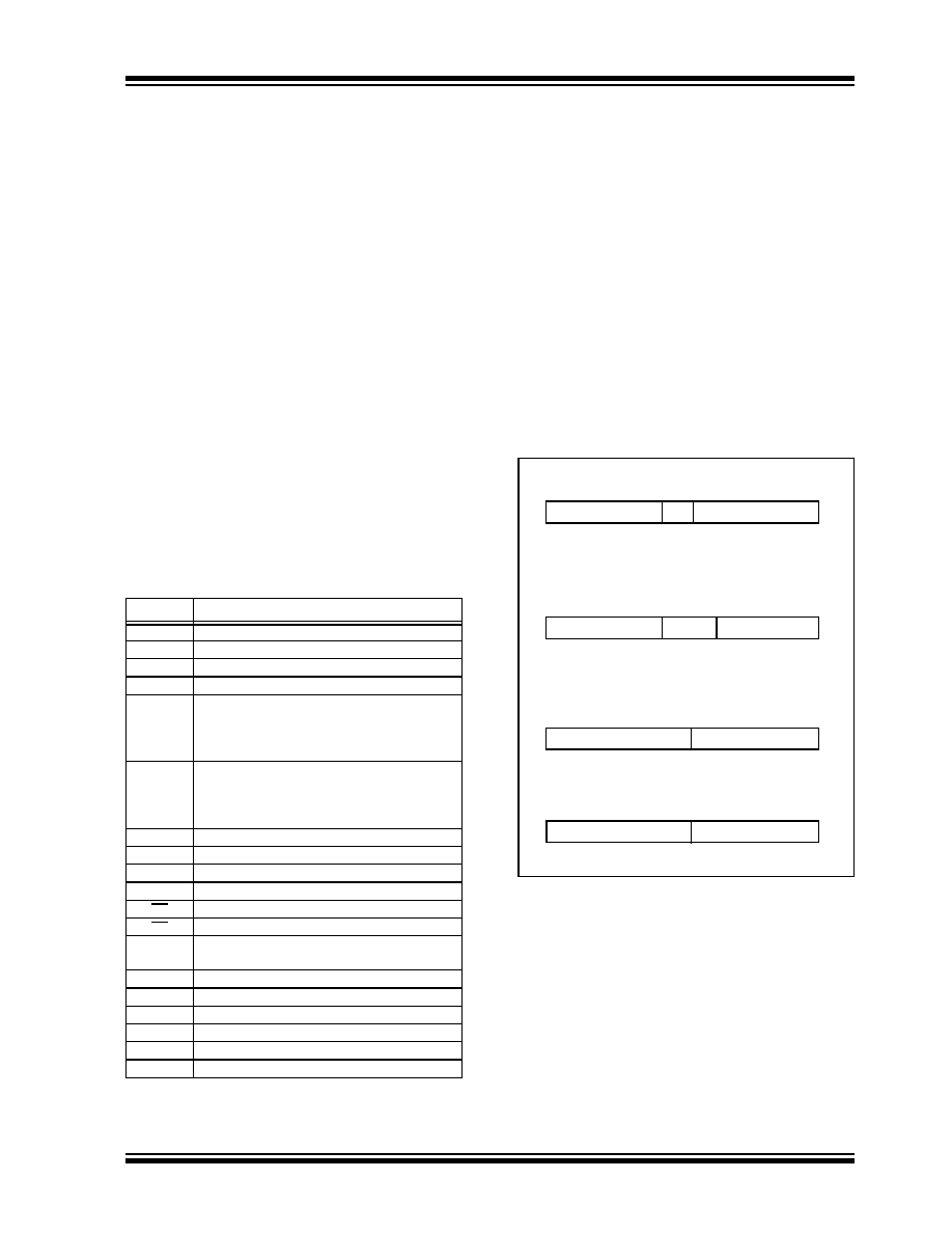
FIGURE 10-1:
GENERAL FORMAT FOR
INSTRUCTIONS
Field
Description
f
Register file address (0x00 to 0x1F)
W
Working register (accumulator)
b
Bit address within an 8-bit file register
k
Literal field, constant data or label
x
Don’t care location (= 0 or 1)
The assembler will generate code with x = 0.
It is the recommended form of use for com-
patibility with all Microchip software tools.
d
Destination select;
d = 0 (store result in W)
d = 1 (store result in file register ’f’)
Default is d = 1
label
Label name
TOS
Top of Stack
PC
Program Counter
WDT
Watchdog Timer Counter
TO
Time-out bit
PD
Power-down bit
dest
Destination, either the W register or the
specified register file location
[
]
Options
(
)
Contents
→
Assigned to
< >
Register bit field
∈
In the set of
italics
User defined term (font is courier)
Byte-oriented file register operations
11
6
5
4
0
d = 0 for destination W
OPCODE
d
f (FILE #)
d = 1 for destination f
f = 5-bit file register address
Bit-oriented file register operations
11
8 7
5 4
0
OPCODE
b (BIT #)
f (FILE #)
b = 3-bit bit address
f = 5-bit file register address
Literal and control operations (except GOTO)
11
8
7
0
OPCODE
k (literal)
k = 8-bit immediate value
Literal and control operations - GOTO instruction
11
9
8
0
OPCODE
k (literal)
k = 9-bit immediate value
相关PDF资料 |
PDF描述 |
|---|---|
| PIC16LF819T-I/SO | IC MCU FLASH 2KX14 EEPROM 18SOIC |
| PIC16LC717/SO | IC MCU OTP 2KX14 A/D PWM 18SOIC |
| PIC16C712-04I/SS | IC MCU OTP 1KX14 A/D PWM 20SSOP |
| PIC12LCE674-04/P | IC MCU OTP 2KX14 LV A/D EE 8DIP |
| VE-25V-IY-B1 | CONVERTER MOD DC/DC 5.8V 50W |
相关代理商/技术参数 |
参数描述 |
|---|---|
| PIC16C55A-40/P | 功能描述:8位微控制器 -MCU .75KB 24 RAM 20 I/O 40MHz PDIP-28 RoHS:否 制造商:Silicon Labs 核心:8051 处理器系列:C8051F39x 数据总线宽度:8 bit 最大时钟频率:50 MHz 程序存储器大小:16 KB 数据 RAM 大小:1 KB 片上 ADC:Yes 工作电源电压:1.8 V to 3.6 V 工作温度范围:- 40 C to + 105 C 封装 / 箱体:QFN-20 安装风格:SMD/SMT |
| PIC16C55A-40/SO | 功能描述:8位微控制器 -MCU .75KB 24 RAM 20 I/O 40MHz SOIC-28 RoHS:否 制造商:Silicon Labs 核心:8051 处理器系列:C8051F39x 数据总线宽度:8 bit 最大时钟频率:50 MHz 程序存储器大小:16 KB 数据 RAM 大小:1 KB 片上 ADC:Yes 工作电源电压:1.8 V to 3.6 V 工作温度范围:- 40 C to + 105 C 封装 / 箱体:QFN-20 安装风格:SMD/SMT |
| PIC16C55A-40/SP | 功能描述:8位微控制器 -MCU .75KB 24 RAM 20 I/O 40MHz SPDIP-28 RoHS:否 制造商:Silicon Labs 核心:8051 处理器系列:C8051F39x 数据总线宽度:8 bit 最大时钟频率:50 MHz 程序存储器大小:16 KB 数据 RAM 大小:1 KB 片上 ADC:Yes 工作电源电压:1.8 V to 3.6 V 工作温度范围:- 40 C to + 105 C 封装 / 箱体:QFN-20 安装风格:SMD/SMT |
| PIC16C55A-40/SS | 功能描述:8位微控制器 -MCU .75KB 24 RAM 20 I/O 40MHz SSOP-28 RoHS:否 制造商:Silicon Labs 核心:8051 处理器系列:C8051F39x 数据总线宽度:8 bit 最大时钟频率:50 MHz 程序存储器大小:16 KB 数据 RAM 大小:1 KB 片上 ADC:Yes 工作电源电压:1.8 V to 3.6 V 工作温度范围:- 40 C to + 105 C 封装 / 箱体:QFN-20 安装风格:SMD/SMT |
| PIC16C55AT-04/SO | 功能描述:8位微控制器 -MCU .75KB 24 RAM 20 I/O 4MHz SOIC-28 RoHS:否 制造商:Silicon Labs 核心:8051 处理器系列:C8051F39x 数据总线宽度:8 bit 最大时钟频率:50 MHz 程序存储器大小:16 KB 数据 RAM 大小:1 KB 片上 ADC:Yes 工作电源电压:1.8 V to 3.6 V 工作温度范围:- 40 C to + 105 C 封装 / 箱体:QFN-20 安装风格:SMD/SMT |
发布紧急采购,3分钟左右您将得到回复。