- 您现在的位置:买卖IC网 > PDF目录11511 > PIC16C55A-20I/SS (Microchip Technology)IC MCU OTP 512X12 28SSOP PDF资料下载
参数资料
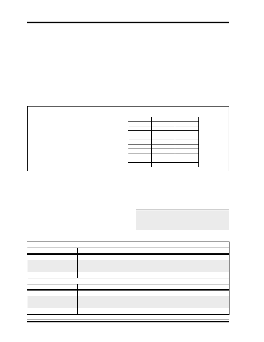
| 型号: | PIC16C55A-20I/SS |
| 厂商: | Microchip Technology |
| 文件页数: | 152/194页 |
| 文件大小: | 0K |
| 描述: | IC MCU OTP 512X12 28SSOP |
| 产品培训模块: | Asynchronous Stimulus |
| 标准包装: | 47 |
| 系列: | PIC® 16C |
| 核心处理器: | PIC |
| 芯体尺寸: | 8-位 |
| 速度: | 20MHz |
| 外围设备: | POR,WDT |
| 输入/输出数: | 20 |
| 程序存储器容量: | 768B(512 x 12) |
| 程序存储器类型: | OTP |
| RAM 容量: | 25 x 8 |
| 电压 - 电源 (Vcc/Vdd): | 3 V ~ 5.5 V |
| 振荡器型: | 外部 |
| 工作温度: | -40°C ~ 85°C |
| 封装/外壳: | 28-SSOP(0.209",5.30mm 宽) |
| 包装: | 管件 |
| 配用: | 309-1026-ND - ADAPTER 28-SSOP TO 28-DIP |
第1页第2页第3页第4页第5页第6页第7页第8页第9页第10页第11页第12页第13页第14页第15页第16页第17页第18页第19页第20页第21页第22页第23页第24页第25页第26页第27页第28页第29页第30页第31页第32页第33页第34页第35页第36页第37页第38页第39页第40页第41页第42页第43页第44页第45页第46页第47页第48页第49页第50页第51页第52页第53页第54页第55页第56页第57页第58页第59页第60页第61页第62页第63页第64页第65页第66页第67页第68页第69页第70页第71页第72页第73页第74页第75页第76页第77页第78页第79页第80页第81页第82页第83页第84页第85页第86页第87页第88页第89页第90页第91页第92页第93页第94页第95页第96页第97页第98页第99页第100页第101页第102页第103页第104页第105页第106页第107页第108页第109页第110页第111页第112页第113页第114页第115页第116页第117页第118页第119页第120页第121页第122页第123页第124页第125页第126页第127页第128页第129页第130页第131页第132页第133页第134页第135页第136页第137页第138页第139页第140页第141页第142页第143页第144页第145页第146页第147页第148页第149页第150页第151页当前第152页第153页第154页第155页第156页第157页第158页第159页第160页第161页第162页第163页第164页第165页第166页第167页第168页第169页第170页第171页第172页第173页第174页第175页第176页第177页第178页第179页第180页第181页第182页第183页第184页第185页第186页第187页第188页第189页第190页第191页第192页第193页第194页
PIC18F2450/4450
DS39760A-page 58
Advance Information
2006 Microchip Technology Inc.
5.2.3
INSTRUCTIONS IN PROGRAM
MEMORY
The
program
memory
is
addressed
in
bytes.
Instructions are stored as two bytes or four bytes in
program memory. The Least Significant Byte of an
instruction word is always stored in a program memory
location with an even address (LSb = 0). To maintain
alignment
with
instruction
boundaries,
the
PC
increments in steps of 2 and the LSb will always read
‘0’ (see Section 5.1.1 “Program Counter”).
Figure 5-4 shows an example of how instruction words
are stored in the program memory.
The CALL and GOTO instructions have the absolute
program
memory
address
embedded
into
the
instruction. Since instructions are always stored on word
boundaries, the data contained in the instruction is a
word address. The word address is written to PC<20:1>,
which accesses the desired byte address in program
memory. Instruction #2 in Figure 5-4 shows how the
instruction, GOTO 0006h, is encoded in the program
memory. Program branch instructions, which encode a
relative address offset, operate in the same manner. The
offset value stored in a branch instruction represents the
number of single-word instructions that the PC will be
offset by. Section 19.0 “Instruction Set Summary”
provides further details of the instruction set.
FIGURE 5-4:
INSTRUCTIONS IN PROGRAM MEMORY
5.2.4
TWO-WORD INSTRUCTIONS
The standard PIC18 instruction set has four two-word
instructions: CALL, MOVFF, GOTO and LSFR. In all
cases, the second word of the instructions always has
‘1111’ as its four Most Significant bits; the other 12 bits
are literal data, usually a data memory address.
The use of ‘1111’ in the 4 MSbs of an instruction
specifies a special form of NOP. If the instruction is
executed in proper sequence, immediately after the
first word, the data in the second word is accessed and
used by the instruction sequence. If the first word is
skipped for some reason and the second word is
executed by itself, a NOP is executed instead. This is
necessary for cases when the two-word instruction is
preceded by a conditional instruction that changes the
PC. Example 5-4 shows how this works.
EXAMPLE 5-4:
TWO-WORD INSTRUCTIONS
Word Address
LSB = 1
LSB = 0
↓
Program Memory
Byte Locations
→
000000h
000002h
000004h
000006h
Instruction 1:
MOVLW
055h
0Fh
55h
000008h
Instruction 2:
GOTO
0006h
EFh
03h
00000Ah
F0h
00h
00000Ch
Instruction 3:
MOVFF
123h, 456h
C1h
23h
00000Eh
F4h
56h
000010h
000012h
000014h
Note:
for
information on two-word instruction in the
extended instruction set.
CASE 1:
Object Code
Source Code
0110 0110 0000 0000
TSTFSZ
REG1
; is RAM location 0?
1100 0001 0010 0011
MOVFF
REG1, REG2
; No, skip this word
1111 0100 0101 0110
; Execute this word as a NOP
0010 0100 0000 0000
ADDWF
REG3
; continue code
CASE 2:
Object Code
Source Code
0110 0110 0000 0000
TSTFSZ
REG1
; is RAM location 0?
1100 0001 0010 0011
MOVFF
REG1, REG2
; Yes, execute this word
1111 0100 0101 0110
; 2nd word of instruction
0010 0100 0000 0000
ADDWF
REG3
; continue code
相关PDF资料 |
PDF描述 |
|---|---|
| PIC16C622A-20E/SS | IC MCU OTP 2KX14 COMP 20SSOP |
| PIC18LF24J50T-I/ML | IC PIC MCU FLASH 16KB 28-QFN |
| PIC18F24J50T-I/ML | IC PIC MCU FLASH 16KB 28-QFN |
| PIC24F32KA301T-I/SS | MCU 32KB FLASH 2KB RAM 20SSOP |
| PIC24FV32KA301T-I/SS | MCU 32KB FLASH 2KB RAM 20SSOP |
相关代理商/技术参数 |
参数描述 |
|---|---|
| PIC16C55A-40/P | 功能描述:8位微控制器 -MCU .75KB 24 RAM 20 I/O 40MHz PDIP-28 RoHS:否 制造商:Silicon Labs 核心:8051 处理器系列:C8051F39x 数据总线宽度:8 bit 最大时钟频率:50 MHz 程序存储器大小:16 KB 数据 RAM 大小:1 KB 片上 ADC:Yes 工作电源电压:1.8 V to 3.6 V 工作温度范围:- 40 C to + 105 C 封装 / 箱体:QFN-20 安装风格:SMD/SMT |
| PIC16C55A-40/SO | 功能描述:8位微控制器 -MCU .75KB 24 RAM 20 I/O 40MHz SOIC-28 RoHS:否 制造商:Silicon Labs 核心:8051 处理器系列:C8051F39x 数据总线宽度:8 bit 最大时钟频率:50 MHz 程序存储器大小:16 KB 数据 RAM 大小:1 KB 片上 ADC:Yes 工作电源电压:1.8 V to 3.6 V 工作温度范围:- 40 C to + 105 C 封装 / 箱体:QFN-20 安装风格:SMD/SMT |
| PIC16C55A-40/SP | 功能描述:8位微控制器 -MCU .75KB 24 RAM 20 I/O 40MHz SPDIP-28 RoHS:否 制造商:Silicon Labs 核心:8051 处理器系列:C8051F39x 数据总线宽度:8 bit 最大时钟频率:50 MHz 程序存储器大小:16 KB 数据 RAM 大小:1 KB 片上 ADC:Yes 工作电源电压:1.8 V to 3.6 V 工作温度范围:- 40 C to + 105 C 封装 / 箱体:QFN-20 安装风格:SMD/SMT |
| PIC16C55A-40/SS | 功能描述:8位微控制器 -MCU .75KB 24 RAM 20 I/O 40MHz SSOP-28 RoHS:否 制造商:Silicon Labs 核心:8051 处理器系列:C8051F39x 数据总线宽度:8 bit 最大时钟频率:50 MHz 程序存储器大小:16 KB 数据 RAM 大小:1 KB 片上 ADC:Yes 工作电源电压:1.8 V to 3.6 V 工作温度范围:- 40 C to + 105 C 封装 / 箱体:QFN-20 安装风格:SMD/SMT |
| PIC16C55AT-04/SO | 功能描述:8位微控制器 -MCU .75KB 24 RAM 20 I/O 4MHz SOIC-28 RoHS:否 制造商:Silicon Labs 核心:8051 处理器系列:C8051F39x 数据总线宽度:8 bit 最大时钟频率:50 MHz 程序存储器大小:16 KB 数据 RAM 大小:1 KB 片上 ADC:Yes 工作电源电压:1.8 V to 3.6 V 工作温度范围:- 40 C to + 105 C 封装 / 箱体:QFN-20 安装风格:SMD/SMT |
发布紧急采购,3分钟左右您将得到回复。