- 您现在的位置:买卖IC网 > PDF目录11349 > PIC16C57-XTI/SS (Microchip Technology)IC MCU OTP 2KX12 28SSOP PDF资料下载
参数资料
| 型号: | PIC16C57-XTI/SS |
| 厂商: | Microchip Technology |
| 文件页数: | 128/194页 |
| 文件大小: | 0K |
| 描述: | IC MCU OTP 2KX12 28SSOP |
| 产品培训模块: | Asynchronous Stimulus |
| 标准包装: | 47 |
| 系列: | PIC® 16C |
| 核心处理器: | PIC |
| 芯体尺寸: | 8-位 |
| 速度: | 4MHz |
| 外围设备: | POR,WDT |
| 输入/输出数: | 20 |
| 程序存储器容量: | 3KB(2K x 12) |
| 程序存储器类型: | OTP |
| RAM 容量: | 72 x 8 |
| 电压 - 电源 (Vcc/Vdd): | 3 V ~ 6.25 V |
| 振荡器型: | 外部 |
| 工作温度: | -40°C ~ 85°C |
| 封装/外壳: | 28-SSOP(0.209",5.30mm 宽) |
| 包装: | 管件 |
| 配用: | 309-1026-ND - ADAPTER 28-SSOP TO 28-DIP |
第1页第2页第3页第4页第5页第6页第7页第8页第9页第10页第11页第12页第13页第14页第15页第16页第17页第18页第19页第20页第21页第22页第23页第24页第25页第26页第27页第28页第29页第30页第31页第32页第33页第34页第35页第36页第37页第38页第39页第40页第41页第42页第43页第44页第45页第46页第47页第48页第49页第50页第51页第52页第53页第54页第55页第56页第57页第58页第59页第60页第61页第62页第63页第64页第65页第66页第67页第68页第69页第70页第71页第72页第73页第74页第75页第76页第77页第78页第79页第80页第81页第82页第83页第84页第85页第86页第87页第88页第89页第90页第91页第92页第93页第94页第95页第96页第97页第98页第99页第100页第101页第102页第103页第104页第105页第106页第107页第108页第109页第110页第111页第112页第113页第114页第115页第116页第117页第118页第119页第120页第121页第122页第123页第124页第125页第126页第127页当前第128页第129页第130页第131页第132页第133页第134页第135页第136页第137页第138页第139页第140页第141页第142页第143页第144页第145页第146页第147页第148页第149页第150页第151页第152页第153页第154页第155页第156页第157页第158页第159页第160页第161页第162页第163页第164页第165页第166页第167页第168页第169页第170页第171页第172页第173页第174页第175页第176页第177页第178页第179页第180页第181页第182页第183页第184页第185页第186页第187页第188页第189页第190页第191页第192页第193页第194页
2002 Microchip Technology Inc.
Preliminary
DS30453D-page 37
PIC16C5X
8.0
TIMER0 MODULE AND TMR0
REGISTER
The Timer0 module has the following features:
8-bit timer/counter register, TMR0
- Readable and writable
8-bit software programmable prescaler
Internal or external clock select
- Edge select for external clock
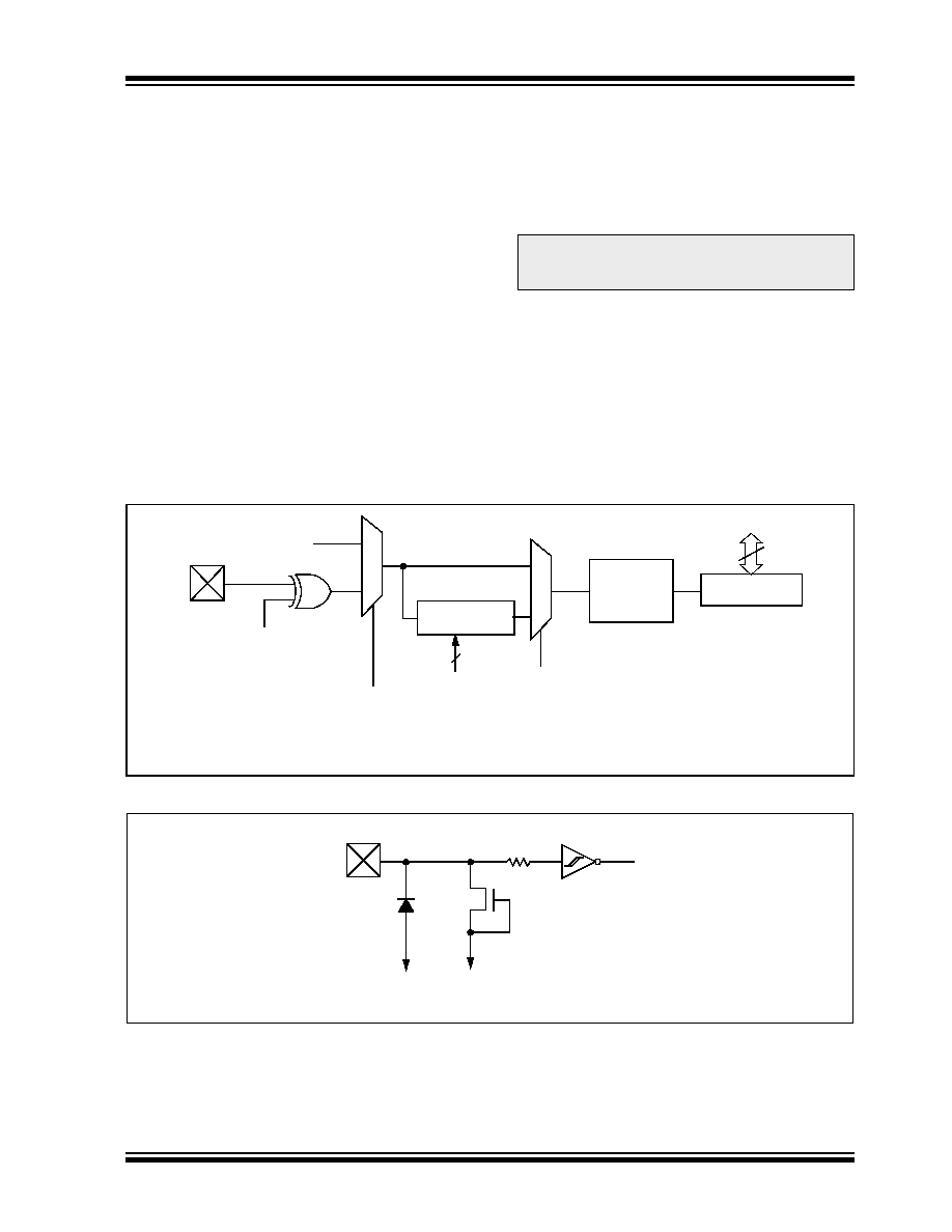
Figure 8-1 is a simplified block diagram of the Timer0
module, while Figure 8-2 shows the electrical structure
of the Timer0 input.
Timer mode is selected by clearing the T0CS bit
(OPTION<5>). In Timer mode, the Timer0 module will
increment every instruction cycle (without prescaler). If
TMR0 register is written, the increment is inhibited for
the following two cycles (Figure 8-3 and Figure 8-4).
The user can work around this by writing an adjusted
value to the TMR0 register.
Counter mode is selected by setting the T0CS bit
(OPTION<5>). In this mode, Timer0 will increment
either on every rising or falling edge of pin T0CKI. The
incrementing edge is determined by the source edge
select bit T0SE (OPTION<4>). Clearing the T0SE bit
selects the rising edge. Restrictions on the external
clock input are discussed in detail in Section 8.1.
The prescaler assignment is controlled in software by
the control bit PSA (OPTION<3>). Clearing the PSA bit
will assign the prescaler to Timer0. The prescaler is not
readable or writable. When the prescaler is assigned to
the Timer0 module, prescale values of 1:2, 1:4,...,
1:256 are selectable. Section 8.2 details the operation
of the prescaler.
A summary of registers associated with the Timer0
module is found in Table 8-1.
FIGURE 8-1:
TIMER0 BLOCK DIAGRAM
FIGURE 8-2:
ELECTRICAL STRUCTURE OF T0CKI PIN
Note:
The prescaler may be used by either the
Timer0 module or the Watchdog Timer, but
not both.
Note 1: Bits T0CS, T0SE, PSA, PS2, PS1 and PS0 are located in the OPTION register
2: The prescaler is shared with the Watchdog Timer (Figure 8-6).
T0CKI
T0SE(1)
0
1
0
pin
T0CS(1)
FOSC/4
Programmable
Prescaler(2)
Sync with
Internal
Clocks
TMR0 reg
PSout
(2 cycle delay)
PSout
Data Bus
8
PSA(1)
PS2, PS1, PS0(1)
3
Sync
VSS
RIN
Schmitt Trigger
N
Input Buffer
T0CKI
pin
Note 1: ESD protection circuits.
(1)
相关PDF资料 |
PDF描述 |
|---|---|
| PIC24HJ32GP302-I/MM | IC PIC MCU FLASH 32K 28-QFN |
| PIC18F2580T-I/ML | IC PIC MCU FLASH 32KX16 28QFN |
| PIC16C622-04E/SS | IC MCU OTP 2KX14 COMP 20SSOP |
| PIC16F876T-04/SO | IC MCU FLASH 8KX14 EE 28SOIC |
| VE-21M-IX-F1 | CONVERTER MOD DC/DC 10V 75W |
相关代理商/技术参数 |
参数描述 |
|---|---|
| PIC16C57XTP | 制造商:MICROCHIP 功能描述:PIC CONTROLLER |
| PIC16C57XTSO | 制造商:MICROCHIP 功能描述:* |
| PIC16C57XTSP | 制造商:MICROCHIP 功能描述:PIC CONTROLLER |
| PIC16C58A/JW | 制造商:Microchip Technology Inc 功能描述: |
| PIC16C58A-04/SO | 制造商:Microchip Technology Inc 功能描述: |
发布紧急采购,3分钟左右您将得到回复。