- 您现在的位置:买卖IC网 > PDF目录10873 > PIC16C716T-20/SS (Microchip Technology)IC MCU OTP 2KX14 A/D PWM 20SSOP PDF资料下载
参数资料
| 型号: | PIC16C716T-20/SS |
| 厂商: | Microchip Technology |
| 文件页数: | 12/106页 |
| 文件大小: | 0K |
| 描述: | IC MCU OTP 2KX14 A/D PWM 20SSOP |
| 标准包装: | 1,600 |
| 系列: | PIC® 16C |
| 核心处理器: | PIC |
| 芯体尺寸: | 8-位 |
| 速度: | 20MHz |
| 外围设备: | 欠压检测/复位,POR,PWM,WDT |
| 输入/输出数: | 13 |
| 程序存储器容量: | 3.5KB(2K x 14) |
| 程序存储器类型: | OTP |
| RAM 容量: | 128 x 8 |
| 电压 - 电源 (Vcc/Vdd): | 4 V ~ 5.5 V |
| 数据转换器: | A/D 4x8b |
| 振荡器型: | 外部 |
| 工作温度: | 0°C ~ 70°C |
| 封装/外壳: | 20-SSOP(0.209",5.30mm 宽) |
| 包装: | 带卷 (TR) |
第1页第2页第3页第4页第5页第6页第7页第8页第9页第10页第11页当前第12页第13页第14页第15页第16页第17页第18页第19页第20页第21页第22页第23页第24页第25页第26页第27页第28页第29页第30页第31页第32页第33页第34页第35页第36页第37页第38页第39页第40页第41页第42页第43页第44页第45页第46页第47页第48页第49页第50页第51页第52页第53页第54页第55页第56页第57页第58页第59页第60页第61页第62页第63页第64页第65页第66页第67页第68页第69页第70页第71页第72页第73页第74页第75页第76页第77页第78页第79页第80页第81页第82页第83页第84页第85页第86页第87页第88页第89页第90页第91页第92页第93页第94页第95页第96页第97页第98页第99页第100页第101页第102页第103页第104页第105页第106页
2005 Microchip Technology Inc.
DS41106B-page 11
PIC16C712/716
2.2.2
SPECIAL FUNCTION REGISTERS
The Special Function Registers are registers used by
the CPU and Peripheral Modules for controlling the
desired operation of the device. These registers are
implemented as static RAM. A list of these registers is
give in Table 2-1.
The Special Function Registers can be classified into
two sets; core (CPU) and peripheral. Those registers
associated with the core functions are described in
detail in this section. Those related to the operation of
the peripheral features are described in detail in that
peripheral feature section.
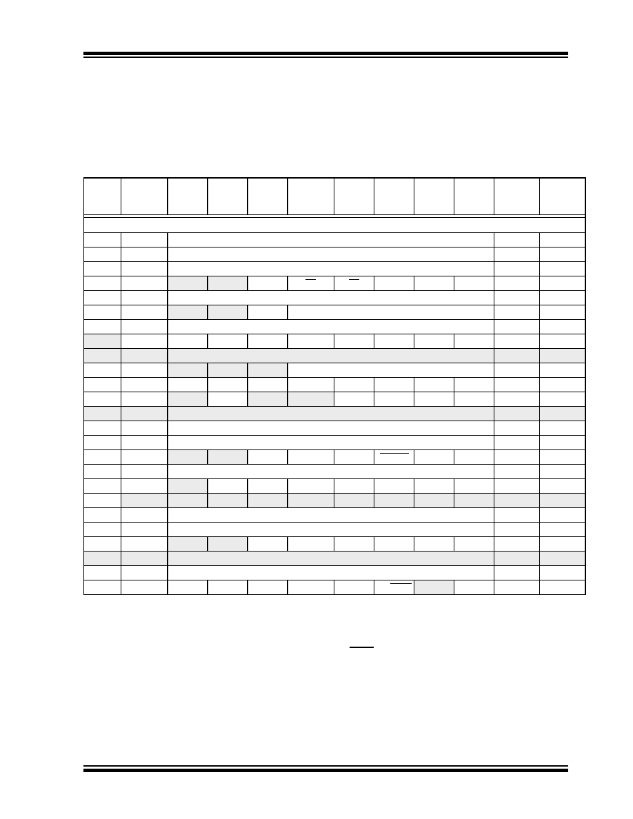
TABLE 2-1:
SPECIAL FUNCTION REGISTER SUMMARY
Addr
Name
Bit 7
Bit 6
Bit 5
Bit 4
Bit 3
Bit 2
Bit 1
Bit 0
Value on:
POR,
BOR
Value on
all other
Resets (4)
Bank 0
00h
INDF(1)
Addressing this location uses contents of FSR to address data memory (not a physical register)
0000 0000
01h
TMR0
Timer0 Module’s Register
xxxx xxxx
uuuu uuuu
02h
PCL(1)
Program Counter’s (PC) Least Significant Byte
0000 0000
03h
STATUS(1)
IRP(4)
RP1(4)
RP0
TO
PD
ZDC
C
rr01 1xxx
rr0q quuu
04h
FSR(1)
Indirect Data Memory Address Pointer
xxxx xxxx
uuuu uuuu
05h
PORTA(5,6)
—
——(7)
PORTA Data Latch when written: PORTA pins when read
--xx xxxx
--xu uuuu
06h
PORTB(5,6)
PORTB Data Latch when written: PORTB pins when read
xxxx xxxx
uuuu uuuu
07h
DATACCP
—(7)
DCCP
—(7)
DT1CK
xxxx xxxx
xxxx xuxu
08h-09h
—
Unimplemented
—
0Ah
PCLATH(1,2)
—
Write Buffer for the upper 5 bits of the Program Counter
---0 0000
0Bh
INTCON(1)
GIE
PEIE
T0IE
INTE
RBIE
T0IF
INTF
RBIF
0000 000x
0000 000u
0Ch
PIR1
—ADIF
—
CCP1IF
TMR2IF
TMR1IF
-0-- 0000
0Dh
—
Unimplemented
—
0Eh
TMR1L
Holding Register for the Least Significant Byte of the 16-bit TMR1 Register
xxxx xxxx
uuuu uuuu
0Fh
TMR1H
Holding Register for the Most Significant Byte of the 16-bit TMR1 Register
xxxx xxxx
uuuu uuuu
10h
T1CON
—
T1CKPS1
T1CKPS0
T1OSCEN
T1SYNC
TMR1CS
TMR1ON
--00 0000
--uu uuuu
11h
TMR2
Timer2 Module’s Register
0000 0000
12h
T2CON
—
TOUTPS3
TOUTPS2
TOUTPS1
TOUTPS0
TMR2ON
T2CKPS1
T2CKPS0
-000 0000
13h-14h
15h
CCPR1L
Capture/Compare/PWM Register1 (LSB)
xxxx xxxx
uuuu uuuu
16h
CCPR1H
Capture/Compare/PWM Register1 (MSB)
xxxx xxxx
uuuu uuuu
17h
CCP1CON
—
DC1B1
DC1B0
CCP1M3
CCP1M2
CCP1M1
CCP1M0
--00 0000
18h-1Dh
—
Unimplemented
—
1Eh
ADRES
A/D Result Register
xxxx xxxx
uuuu uuuu
1Fh
ADCON0
ADCS1
ADCS0
CHS2
CHS1
CHS0
GO/DONE
—ADON
0000 00-0
Legend: x = unknown, u = unchanged, q = value depends on condition, — = unimplemented, read as ‘0’,
Shaded locations are unimplemented, read as ‘0’.
Note 1: These registers can be addressed from either bank.
2:
The upper byte of the program counter is not directly accessible. PCLATH is a holding register for PC<12:8> whose contents
are transferred to the upper byte of the program counter.
3:
Other (non Power-up) Resets include: external Reset through MCLR and the Watchdog Timer Reset.
4:
The IRP and RP1 bits are reserved. Always maintain these bits clear.
5:
On any device Reset, these pins are configured as inputs.
6:
This is the value that will be in the port output latch.
7:
Reserved bits; Do Not Use.
相关PDF资料 |
PDF描述 |
|---|---|
| VE-21F-CU-F2 | CONVERTER MOD DC/DC 72V 200W |
| PIC16C716T-20E/SS | IC MCU OTP 2KX14 A/D PWM 20SSOP |
| PIC16C716T-20E/SO | IC MCU OTP 2KX14 A/D PWM 18SOIC |
| PIC16C716T-04/SS | IC MCU OTP 2KX14 A/D PWM 20SSOP |
| PIC16C716T-04/SO | IC MCU OTP 2KX14 A/D PWM 18SOIC |
相关代理商/技术参数 |
参数描述 |
|---|---|
| PIC16C717/JW | 功能描述:8位微控制器 -MCU 3.5KB 256 RAM 16 I/O RoHS:否 制造商:Silicon Labs 核心:8051 处理器系列:C8051F39x 数据总线宽度:8 bit 最大时钟频率:50 MHz 程序存储器大小:16 KB 数据 RAM 大小:1 KB 片上 ADC:Yes 工作电源电压:1.8 V to 3.6 V 工作温度范围:- 40 C to + 105 C 封装 / 箱体:QFN-20 安装风格:SMD/SMT |
| PIC16C717/P | 功能描述:8位微控制器 -MCU 3.5KB 256 RAM 16 I/O RoHS:否 制造商:Silicon Labs 核心:8051 处理器系列:C8051F39x 数据总线宽度:8 bit 最大时钟频率:50 MHz 程序存储器大小:16 KB 数据 RAM 大小:1 KB 片上 ADC:Yes 工作电源电压:1.8 V to 3.6 V 工作温度范围:- 40 C to + 105 C 封装 / 箱体:QFN-20 安装风格:SMD/SMT |
| PIC16C717/P | 制造商:Microchip Technology Inc 功能描述:IC 8BIT CMOS MCU 16C717 DIP18 |
| PIC16C717/P | 制造商:Microchip Technology Inc 功能描述:Microcontroller IC Number of I/Os:16 |
| PIC16C717/PC01 | 制造商:Microchip Technology Inc 功能描述: |
发布紧急采购,3分钟左右您将得到回复。