- 您现在的位置:买卖IC网 > PDF目录3810 > PIC16C74A-20/P (Microchip Technology)IC MCU OTP 4KX14 A/D PWM 40DIP PDF资料下载
参数资料
| 型号: | PIC16C74A-20/P |
| 厂商: | Microchip Technology |
| 文件页数: | 11/114页 |
| 文件大小: | 0K |
| 描述: | IC MCU OTP 4KX14 A/D PWM 40DIP |
| 产品培训模块: | Asynchronous Stimulus 8-bit PIC® Microcontroller Portfolio |
| 标准包装: | 10 |
| 系列: | PIC® 16C |
| 核心处理器: | PIC |
| 芯体尺寸: | 8-位 |
| 速度: | 20MHz |
| 连通性: | I²C,SPI,UART/USART |
| 外围设备: | 欠压检测/复位,POR,PWM,WDT |
| 输入/输出数: | 33 |
| 程序存储器容量: | 7KB(4K x 14) |
| 程序存储器类型: | OTP |
| RAM 容量: | 192 x 8 |
| 电压 - 电源 (Vcc/Vdd): | 4 V ~ 6 V |
| 数据转换器: | A/D 8x8b |
| 振荡器型: | 外部 |
| 工作温度: | 0°C ~ 70°C |
| 封装/外壳: | 40-DIP(0.600",15.24mm) |
| 包装: | 管件 |
| 配用: | 444-1001-ND - DEMO BOARD FOR PICMICRO MCU |
第1页第2页第3页第4页第5页第6页第7页第8页第9页第10页当前第11页第12页第13页第14页第15页第16页第17页第18页第19页第20页第21页第22页第23页第24页第25页第26页第27页第28页第29页第30页第31页第32页第33页第34页第35页第36页第37页第38页第39页第40页第41页第42页第43页第44页第45页第46页第47页第48页第49页第50页第51页第52页第53页第54页第55页第56页第57页第58页第59页第60页第61页第62页第63页第64页第65页第66页第67页第68页第69页第70页第71页第72页第73页第74页第75页第76页第77页第78页第79页第80页第81页第82页第83页第84页第85页第86页第87页第88页第89页第90页第91页第92页第93页第94页第95页第96页第97页第98页第99页第100页第101页第102页第103页第104页第105页第106页第107页第108页第109页第110页第111页第112页第113页第114页
PIC16C7X
DS30390E-page 108
1997 Microchip Technology Inc.
12.2.2
USART ASYNCHRONOUS RECEIVER
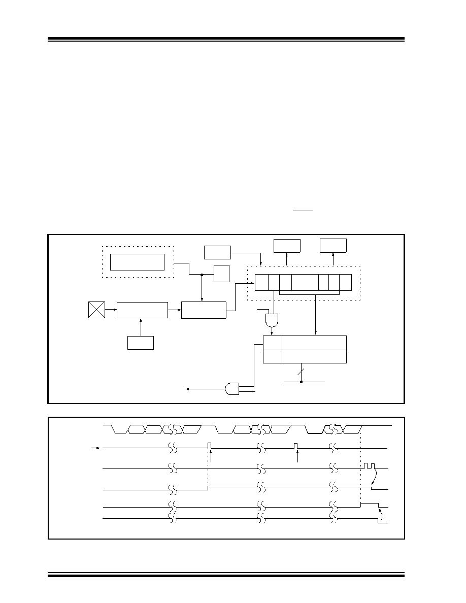
The receiver block diagram is shown in Figure 12-10.
The data is received on the RC7/RX/DT pin and drives
the data recovery block. The data recovery block is
actually a high speed shifter operating at x16 times the
baud rate, whereas the main receive serial shifter oper-
ates at the bit rate or at FOSC.
Once Asynchronous mode is selected, reception is
enabled by setting bit CREN (RCSTA<4>).
The heart of the receiver is the receive (serial) shift reg-
ister (RSR). After sampling the STOP bit, the received
data in the RSR is transferred to the RCREG register (if
it is empty). If the transfer is complete, ag bit RCIF
(PIR1<5>) is set. The actual interrupt can be enabled/
disabled
by
setting/clearing
enable
bit
RCIE
(PIE1<5>). Flag bit RCIF is a read only bit which is
cleared by the hardware. It is cleared when the RCREG
register has been read and is empty. The RCREG is a
double buffered register, i.e. it is a two deep FIFO. It is
possible for two bytes of data to be received and trans-
ferred to the RCREG FIFO and a third byte begin shift-
ing to the RSR register. On the detection of the STOP
bit of the third byte, if the RCREG register is still full
then overrun error bit OERR (RCSTA<1>) will be set.
The word in the RSR will be lost. The RCREG register
can be read twice to retrieve the two bytes in the FIFO.
Overrun bit OERR has to be cleared in software. This
is done by resetting the receive logic (CREN is cleared
and then set). If bit OERR is set, transfers from the
RSR register to the RCREG register are inhibited, so it
is essential to clear error bit OERR if it is set. Framing
error bit FERR (RCSTA<2>) is set if a stop bit is
detected as clear. Bit FERR and the 9th receive bit are
buffered the same way as the receive data. Reading
the RCREG, will load bits RX9D and FERR with new
values, therefore it is essential for the user to read the
RCSTA register before reading RCREG register in
order not to lose the old FERR and RX9D information.
FIGURE 12-10: USART RECEIVE BLOCK DIAGRAM
FIGURE 12-11: ASYNCHRONOUS RECEPTION
x64 Baud Rate CLK
SPBRG
Baud Rate Generator
RC7/RX/DT
Pin Buffer
and Control
SPEN
Data
Recovery
CREN
OERR
FERR
RSR register
MSb
LSb
RX9D
RCREG register
FIFO
Interrupt
RCIF
RCIE
Data Bus
8
÷ 64
÷ 16
or
Stop
Start
(8)
7
1
0
RX9
Start
bit
bit7/8
bit1
bit0
bit7/8
bit0
Stop
bit
Start
bit
Start
bit
bit7/8
Stop
bit
RX (pin)
reg
Rcv buffer reg
Rcv shift
Read Rcv
buffer reg
RCREG
RCIF
(interrupt ag)
OERR bit
CREN
WORD 1
RCREG
WORD 2
RCREG
Stop
bit
Note: This timing diagram shows three words appearing on the RX input. The RCREG (receive buffer) is read after the third word,
causing the OERR (overrun) bit to be set.
相关PDF资料 |
PDF描述 |
|---|---|
| PIC16LF877-04I/L | IC MCU FLASH 8KX14 EE A/D 44PLCC |
| PIC24EP256GU810-I/BG | IC DSC 16B 256KB FLASH 121TFBGA |
| DSPIC33EP256MU810-I/BG | IC DSC 16BIT 256KB 121XBGA |
| 516-230-512 | COVER METAL RACK & PANEL 120POS |
| 516-230-590 | COVER METAL RACK & PANEL 90POS |
相关代理商/技术参数 |
参数描述 |
|---|---|
| PIC16C74AT-04/L | 功能描述:8位微控制器 -MCU 7KB 192 RAM 33 I/O RoHS:否 制造商:Silicon Labs 核心:8051 处理器系列:C8051F39x 数据总线宽度:8 bit 最大时钟频率:50 MHz 程序存储器大小:16 KB 数据 RAM 大小:1 KB 片上 ADC:Yes 工作电源电压:1.8 V to 3.6 V 工作温度范围:- 40 C to + 105 C 封装 / 箱体:QFN-20 安装风格:SMD/SMT |
| PIC16C74AT-04/PQ | 功能描述:8位微控制器 -MCU 7KB 192 RAM 33 I/O RoHS:否 制造商:Silicon Labs 核心:8051 处理器系列:C8051F39x 数据总线宽度:8 bit 最大时钟频率:50 MHz 程序存储器大小:16 KB 数据 RAM 大小:1 KB 片上 ADC:Yes 工作电源电压:1.8 V to 3.6 V 工作温度范围:- 40 C to + 105 C 封装 / 箱体:QFN-20 安装风格:SMD/SMT |
| PIC16C74AT-04/PT | 功能描述:8位微控制器 -MCU 7KB 192 RAM 33 I/O RoHS:否 制造商:Silicon Labs 核心:8051 处理器系列:C8051F39x 数据总线宽度:8 bit 最大时钟频率:50 MHz 程序存储器大小:16 KB 数据 RAM 大小:1 KB 片上 ADC:Yes 工作电源电压:1.8 V to 3.6 V 工作温度范围:- 40 C to + 105 C 封装 / 箱体:QFN-20 安装风格:SMD/SMT |
| PIC16C74AT-04E/L | 功能描述:8位微控制器 -MCU 7KB 192 RAM 33 I/O RoHS:否 制造商:Silicon Labs 核心:8051 处理器系列:C8051F39x 数据总线宽度:8 bit 最大时钟频率:50 MHz 程序存储器大小:16 KB 数据 RAM 大小:1 KB 片上 ADC:Yes 工作电源电压:1.8 V to 3.6 V 工作温度范围:- 40 C to + 105 C 封装 / 箱体:QFN-20 安装风格:SMD/SMT |
| PIC16C74AT-04E/PQ | 功能描述:8位微控制器 -MCU 7KB 192 RAM 33 I/O RoHS:否 制造商:Silicon Labs 核心:8051 处理器系列:C8051F39x 数据总线宽度:8 bit 最大时钟频率:50 MHz 程序存储器大小:16 KB 数据 RAM 大小:1 KB 片上 ADC:Yes 工作电源电压:1.8 V to 3.6 V 工作温度范围:- 40 C to + 105 C 封装 / 箱体:QFN-20 安装风格:SMD/SMT |
发布紧急采购,3分钟左右您将得到回复。