- 您现在的位置:买卖IC网 > PDF目录3832 > PIC16C924-04/L (Microchip Technology)IC MCU OTP 4KX14 LCD DVR 68PLCC PDF资料下载
参数资料
| 型号: | PIC16C924-04/L |
| 厂商: | Microchip Technology |
| 文件页数: | 93/115页 |
| 文件大小: | 0K |
| 描述: | IC MCU OTP 4KX14 LCD DVR 68PLCC |
| 产品培训模块: | Asynchronous Stimulus 8-bit PIC® Microcontroller Portfolio |
| 标准包装: | 19 |
| 系列: | PIC® 16C |
| 核心处理器: | PIC |
| 芯体尺寸: | 8-位 |
| 速度: | 4MHz |
| 连通性: | I²C,SPI |
| 外围设备: | LCD,POR,PWM,WDT |
| 输入/输出数: | 25 |
| 程序存储器容量: | 7KB(4K x 14) |
| 程序存储器类型: | OTP |
| RAM 容量: | 176 x 8 |
| 电压 - 电源 (Vcc/Vdd): | 4 V ~ 6 V |
| 数据转换器: | A/D 5x8b |
| 振荡器型: | 外部 |
| 工作温度: | 0°C ~ 70°C |
| 封装/外壳: | 68-LCC(J 形引线) |
| 包装: | 管件 |
| 配用: | AC164308-ND - MODULE SKT FOR PM3 68PLCC DVA16XL680-ND - ADAPTER DEVICE FOR MPLAB-ICE AC164024-ND - ADAPTER PICSTART PLUS 68PLCC |
第1页第2页第3页第4页第5页第6页第7页第8页第9页第10页第11页第12页第13页第14页第15页第16页第17页第18页第19页第20页第21页第22页第23页第24页第25页第26页第27页第28页第29页第30页第31页第32页第33页第34页第35页第36页第37页第38页第39页第40页第41页第42页第43页第44页第45页第46页第47页第48页第49页第50页第51页第52页第53页第54页第55页第56页第57页第58页第59页第60页第61页第62页第63页第64页第65页第66页第67页第68页第69页第70页第71页第72页第73页第74页第75页第76页第77页第78页第79页第80页第81页第82页第83页第84页第85页第86页第87页第88页第89页第90页第91页第92页当前第93页第94页第95页第96页第97页第98页第99页第100页第101页第102页第103页第104页第105页第106页第107页第108页第109页第110页第111页第112页第113页第114页第115页
1997 Microchip Technology Inc.
DS30444E - page 79
PIC16C9XX
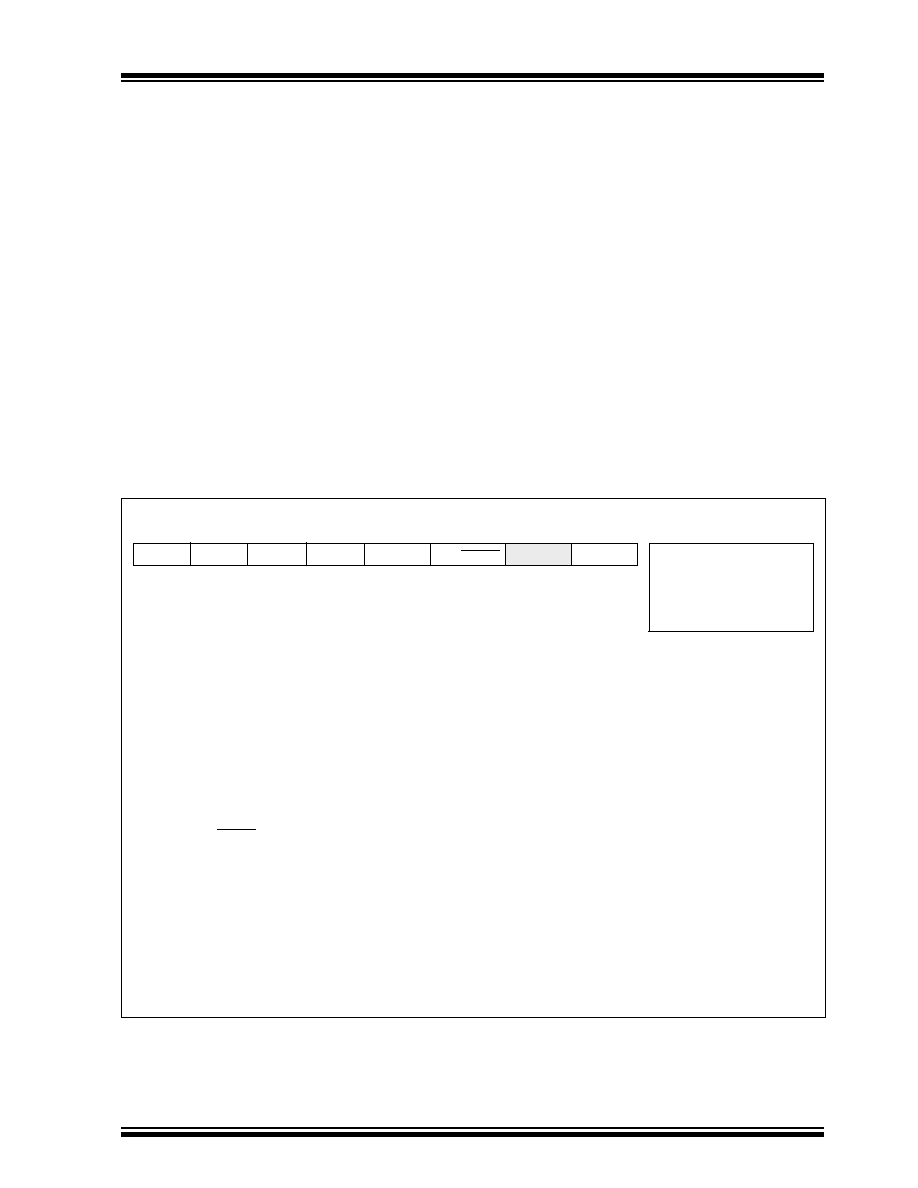
FIGURE 12-1: ADCON0 REGISTER (ADDRESS 1Fh)
R/W-0
ADCS1 ADCS0
CHS2
CHS1
CHS0
GO/DONE
—
ADON
R = Readable bit
W = Writable bit
U = Unimplemented bit,
read as ‘0’
- n = Value at POR reset
bit7
bit0
bit 7-6:
ADCS1:ADCS0: A/D Conversion Clock Select bits
00
= FOSC/2
01
= FOSC/8
10
= FOSC/32
11
= FRC (clock derived from an RC oscillation)
bit 5-3: CHS2:CHS0: Analog Channel Select bits
000
= channel 0, (RA0/AN0)
001
= channel 1, (RA1/AN1)
010
= channel 2, (RA2/AN2)
011
= channel 3, (RA3/AN3)
100
= channel 4, (RA5/AN4)
bit 2:
GO/DONE: A/D Conversion Status bit
If ADON = 1
1 = A/D conversion in progress (setting this bit starts the A/D conversion)
0 = A/D conversion not in progress (This bit is automatically cleared by hardware when the A/D conversion
is complete)
bit 1:
Reserved: Always maintain this bit clear
bit 0:
ADON: A/D On bit
1 = A/D converter module is operating
0 = A/D converter module is shutoff and consumes no operating current
12.0
ANALOG-TO-DIGITAL
CONVERTER (A/D) MODULE
This section applies to the PIC16C924 only.
The analog-to-digital (A/D) converter module has ve
inputs.
The A/D allows conversion of an analog input signal to
a corresponding 8-bit digital number (refer to Applica-
tion Note AN546 for use of A/D Converter). The output
of the sample and hold is the input into the converter,
which generates the result via successive approxima-
tion. The analog reference voltage is software select-
able to either the device’s AVDD pin or the voltage level
on the RA3/AN3/VREF pin. The A/D converter has a
unique feature of being able to operate while the device
is in SLEEP mode.
To operate in sleep, the A/D conversion clock must be
derived from the A/D’s internal RC oscillator.
The A/D module has three registers. These registers
are:
A/D Result Register (ADRES)
A/D Control Register 0 (ADCON0)
A/D Control Register 1 (ADCON1)
The ADCON0 register, shown in Figure 12-1, controls
the operation of the A/D module. The ADCON1 regis-
ter, shown in Figure 12-2, congures the functions of
the port pins. The port pins can be congured as ana-
log inputs (RA3 can also be a voltage reference) or as
digital I/O.
相关PDF资料 |
PDF描述 |
|---|---|
| PIC16F767-I/SO | IC PIC MCU FLASH 8KX14 28SOIC |
| PIC24FJ64GA310-I/PF | MCU 16BIT 64KB FLASH 100TQFP |
| DSPIC33FJ64GP202-E/MM | IC DSPIC MCU/DSP 64K 28-QFN |
| PIC16F876A-I/ML | IC MCU FLASH 8KX14 A/D 28QFN |
| PIC16F876A-I/SO | IC MCU FLASH 8KX14 EE 28SOIC |
相关代理商/技术参数 |
参数描述 |
|---|---|
| PIC16C924-08/L | 功能描述:8位微控制器 -MCU 7KB 176 RAM 52 I/O RoHS:否 制造商:Silicon Labs 核心:8051 处理器系列:C8051F39x 数据总线宽度:8 bit 最大时钟频率:50 MHz 程序存储器大小:16 KB 数据 RAM 大小:1 KB 片上 ADC:Yes 工作电源电压:1.8 V to 3.6 V 工作温度范围:- 40 C to + 105 C 封装 / 箱体:QFN-20 安装风格:SMD/SMT |
| PIC16C924-08/PT | 功能描述:8位微控制器 -MCU 7KB 176 RAM 52 I/O RoHS:否 制造商:Silicon Labs 核心:8051 处理器系列:C8051F39x 数据总线宽度:8 bit 最大时钟频率:50 MHz 程序存储器大小:16 KB 数据 RAM 大小:1 KB 片上 ADC:Yes 工作电源电压:1.8 V to 3.6 V 工作温度范围:- 40 C to + 105 C 封装 / 箱体:QFN-20 安装风格:SMD/SMT |
| PIC16C924-08I/L | 功能描述:8位微控制器 -MCU 7KB 176 RAM 52 I/O RoHS:否 制造商:Silicon Labs 核心:8051 处理器系列:C8051F39x 数据总线宽度:8 bit 最大时钟频率:50 MHz 程序存储器大小:16 KB 数据 RAM 大小:1 KB 片上 ADC:Yes 工作电源电压:1.8 V to 3.6 V 工作温度范围:- 40 C to + 105 C 封装 / 箱体:QFN-20 安装风格:SMD/SMT |
| PIC16C924-08I/PT | 功能描述:8位微控制器 -MCU 7KB 176 RAM 52 I/O RoHS:否 制造商:Silicon Labs 核心:8051 处理器系列:C8051F39x 数据总线宽度:8 bit 最大时钟频率:50 MHz 程序存储器大小:16 KB 数据 RAM 大小:1 KB 片上 ADC:Yes 工作电源电压:1.8 V to 3.6 V 工作温度范围:- 40 C to + 105 C 封装 / 箱体:QFN-20 安装风格:SMD/SMT |
| PIC16C924CL | 制造商:MICROCHIP 功能描述:New |
发布紧急采购,3分钟左右您将得到回复。