- 您现在的位置:买卖IC网 > PDF目录11343 > PIC16C924-04I/PT (Microchip Technology)IC MCU OTP 4KX14 LCD DVR 64TQFP PDF资料下载
参数资料
| 型号: | PIC16C924-04I/PT |
| 厂商: | Microchip Technology |
| 文件页数: | 82/115页 |
| 文件大小: | 0K |
| 描述: | IC MCU OTP 4KX14 LCD DVR 64TQFP |
| 产品培训模块: | Asynchronous Stimulus |
| 标准包装: | 160 |
| 系列: | PIC® 16C |
| 核心处理器: | PIC |
| 芯体尺寸: | 8-位 |
| 速度: | 4MHz |
| 连通性: | I²C,SPI |
| 外围设备: | LCD,POR,PWM,WDT |
| 输入/输出数: | 25 |
| 程序存储器容量: | 7KB(4K x 14) |
| 程序存储器类型: | OTP |
| RAM 容量: | 176 x 8 |
| 电压 - 电源 (Vcc/Vdd): | 4 V ~ 6 V |
| 数据转换器: | A/D 5x8b |
| 振荡器型: | 外部 |
| 工作温度: | -40°C ~ 85°C |
| 封装/外壳: | 64-TQFP |
| 包装: | 托盘 |
| 配用: | DVA16PQ640-ND - ADAPTER DEVICE FOR MPLAB-ICE AC164023-ND - MODULE SKT PROMATEII 68TQFP |
第1页第2页第3页第4页第5页第6页第7页第8页第9页第10页第11页第12页第13页第14页第15页第16页第17页第18页第19页第20页第21页第22页第23页第24页第25页第26页第27页第28页第29页第30页第31页第32页第33页第34页第35页第36页第37页第38页第39页第40页第41页第42页第43页第44页第45页第46页第47页第48页第49页第50页第51页第52页第53页第54页第55页第56页第57页第58页第59页第60页第61页第62页第63页第64页第65页第66页第67页第68页第69页第70页第71页第72页第73页第74页第75页第76页第77页第78页第79页第80页第81页当前第82页第83页第84页第85页第86页第87页第88页第89页第90页第91页第92页第93页第94页第95页第96页第97页第98页第99页第100页第101页第102页第103页第104页第105页第106页第107页第108页第109页第110页第111页第112页第113页第114页第115页
1997 Microchip Technology Inc.
DS30444E - page 69
PIC16C9XX
11.2
I2C
Overview
This section provides an overview of the Inter-Inte-
the operation of the SSP module in I2C mode.
The I2C bus is a two-wire serial interface developed by
the Philips Corporation. The original specication, or
standard mode, was for data transfers of up to 100
Kbps. An enhanced specication, or fast mode is not
supported. This device will communicate with fast
mode devices if attached to the same bus.
The I2C interface employs a comprehensive protocol to
ensure reliable transmission and reception of data.
When transmitting data, one device is the “master”
which initiates transfer on the bus and generates the
clock signals to permit that transfer, while the other
device(s) acts as the “slave.” All portions of the slave
protocol are implemented in the SSP module’s hard-
ware, except general call support, while portions of the
master protocol need to be addressed in the
PIC16CXXX software. Table 11-2 denes some of the
I2C bus terminology. For additional information on the
I2C interface specication, refer to the Philips docu-
ment “
The I2C bus and how to use it.” #939839340011,
which can be obtained from the Philips Corporation.
In the I2C interface protocol each device has an
address. When a master wishes to initiate a data trans-
fer, it rst transmits the address of the device that it
wishes to “talk” to. All devices “listen” to see if this is
their address. Within this address, a bit species if the
master wishes to read-from/write-to the slave device.
The master and slave are always in opposite modes
(transmitter/receiver) of operation during a data trans-
fer. That is they can be thought of as operating in either
of these two relations:
Master-transmitter and Slave-receiver
Slave-transmitter and Master-receiver
In both cases the master generates the clock signal.
The output stages of the clock (SCL) and data (SDA)
lines must have an open-drain or open-collector in
order to perform the wired-AND function of the bus.
External pull-up resistors are used to ensure a high
level when no device is pulling the line down. The num-
ber of devices that may be attached to the I2C bus is
limited only by the maximum bus loading specication
of 400 pF.
11.2.1
INITIATING AND TERMINATING DATA
TRANSFER
During times of no data transfer (idle time), both the
clock line (SCL) and the data line (SDA) are pulled high
through the external pull-up resistors. The START and
STOP conditions determine the start and stop of data
transmission. The START condition is dened as a high
to low transition of the SDA when the SCL is high. The
STOP condition is dened as a low to high transition of
the SDA when the SCL is high. Figure 11-8 shows the
START and STOP conditions. The master generates
these conditions for starting and terminating data trans-
fer. Due to the denition of the START and STOP con-
ditions, when data is being transmitted, the SDA line
can only change state when the SCL line is low.
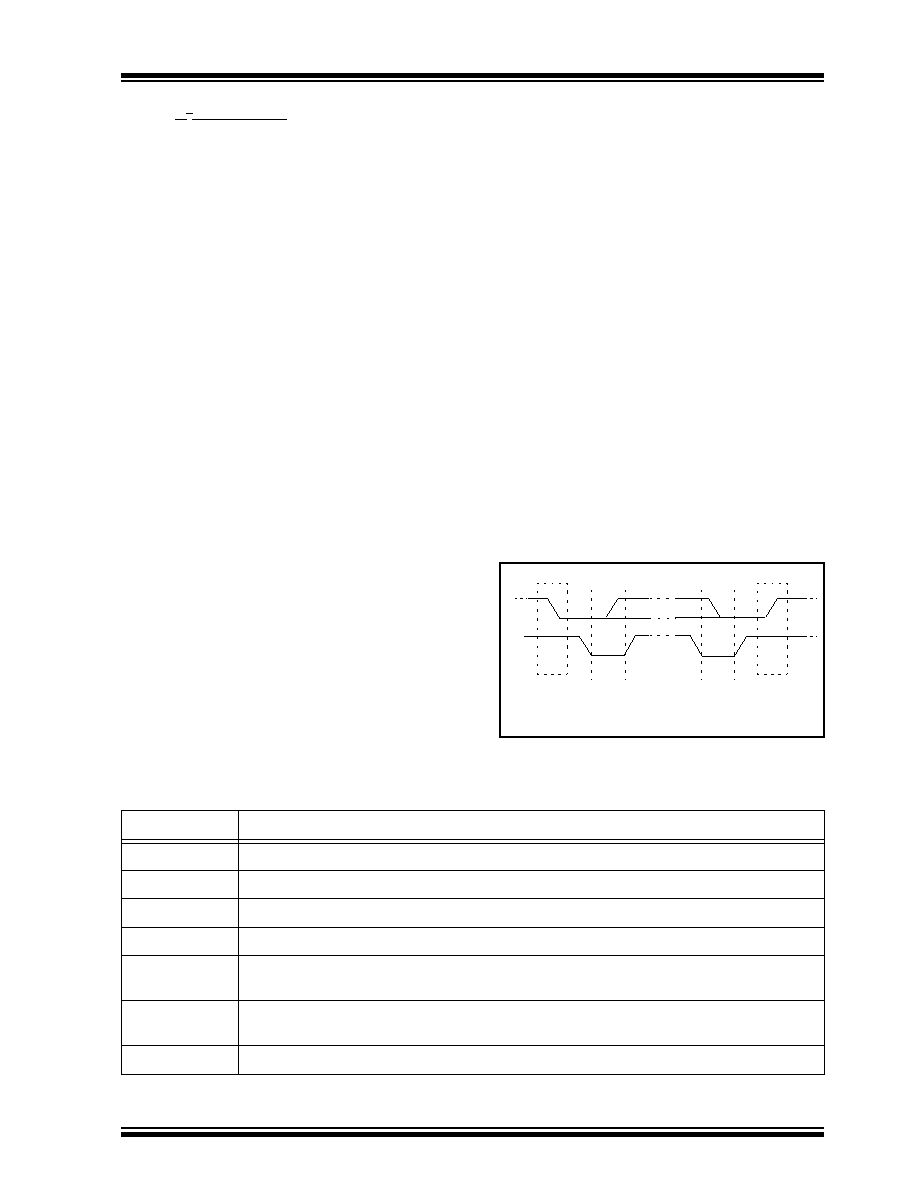
FIGURE 11-8: START AND STOP
CONDITIONS
SDA
SCL
S
P
Start
Condition
Change
of Data
Allowed
Change
of Data
Allowed
Stop
Condition
TABLE 11-2: I2C BUS TERMINOLOGY
Term
Description
Transmitter
The device that sends the data to the bus.
Receiver
The device that receives the data from the bus.
Master
The device which initiates the transfer, generates the clock and terminates the transfer.
Slave
The device addressed by a master.
Multi-master
More than one master device in a system. These masters can attempt to control the bus at the
same time without corrupting the message.
Arbitration
Procedure that ensures that only one of the master devices will control the bus. This ensure that
the transfer data does not get corrupted.
Synchronization
Procedure where the clock signals of two or more devices are synchronized.
相关PDF资料 |
PDF描述 |
|---|---|
| ISL54209IRUZ-T7A | IC USB SWITCH DUAL SPDT 10UTQFN |
| PIC16LF874-04/P | IC MCU FLASH 4KX14 EE A/D 40DIP |
| PIC16C621-20/SO | IC MCU OTP 1KX14 COMP 18SOIC |
| PIC16F873T-20/SO | IC MCU FLASH 4KX14 EE 28SOIC |
| PIC16F767-E/ML | IC PIC MCU FLASH 8KX14 28QFN |
相关代理商/技术参数 |
参数描述 |
|---|---|
| PIC16C924-08/L | 功能描述:8位微控制器 -MCU 7KB 176 RAM 52 I/O RoHS:否 制造商:Silicon Labs 核心:8051 处理器系列:C8051F39x 数据总线宽度:8 bit 最大时钟频率:50 MHz 程序存储器大小:16 KB 数据 RAM 大小:1 KB 片上 ADC:Yes 工作电源电压:1.8 V to 3.6 V 工作温度范围:- 40 C to + 105 C 封装 / 箱体:QFN-20 安装风格:SMD/SMT |
| PIC16C924-08/PT | 功能描述:8位微控制器 -MCU 7KB 176 RAM 52 I/O RoHS:否 制造商:Silicon Labs 核心:8051 处理器系列:C8051F39x 数据总线宽度:8 bit 最大时钟频率:50 MHz 程序存储器大小:16 KB 数据 RAM 大小:1 KB 片上 ADC:Yes 工作电源电压:1.8 V to 3.6 V 工作温度范围:- 40 C to + 105 C 封装 / 箱体:QFN-20 安装风格:SMD/SMT |
| PIC16C924-08I/L | 功能描述:8位微控制器 -MCU 7KB 176 RAM 52 I/O RoHS:否 制造商:Silicon Labs 核心:8051 处理器系列:C8051F39x 数据总线宽度:8 bit 最大时钟频率:50 MHz 程序存储器大小:16 KB 数据 RAM 大小:1 KB 片上 ADC:Yes 工作电源电压:1.8 V to 3.6 V 工作温度范围:- 40 C to + 105 C 封装 / 箱体:QFN-20 安装风格:SMD/SMT |
| PIC16C924-08I/PT | 功能描述:8位微控制器 -MCU 7KB 176 RAM 52 I/O RoHS:否 制造商:Silicon Labs 核心:8051 处理器系列:C8051F39x 数据总线宽度:8 bit 最大时钟频率:50 MHz 程序存储器大小:16 KB 数据 RAM 大小:1 KB 片上 ADC:Yes 工作电源电压:1.8 V to 3.6 V 工作温度范围:- 40 C to + 105 C 封装 / 箱体:QFN-20 安装风格:SMD/SMT |
| PIC16C924CL | 制造商:MICROCHIP 功能描述:New |
发布紧急采购,3分钟左右您将得到回复。