- 您现在的位置:买卖IC网 > PDF目录3865 > PIC16CE625-04/P (Microchip Technology)IC MCU OTP 2KX14 EE COMP 18DIP PDF资料下载
参数资料
| 型号: | PIC16CE625-04/P |
| 厂商: | Microchip Technology |
| 文件页数: | 51/100页 |
| 文件大小: | 0K |
| 描述: | IC MCU OTP 2KX14 EE COMP 18DIP |
| 产品培训模块: | Asynchronous Stimulus 8-bit PIC® Microcontroller Portfolio |
| 标准包装: | 25 |
| 系列: | PIC® 16C |
| 核心处理器: | PIC |
| 芯体尺寸: | 8-位 |
| 速度: | 4MHz |
| 外围设备: | 欠压检测/复位,POR,WDT |
| 输入/输出数: | 13 |
| 程序存储器容量: | 3.5KB(2K x 14) |
| 程序存储器类型: | OTP |
| EEPROM 大小: | 128 x 8 |
| RAM 容量: | 128 x 8 |
| 电压 - 电源 (Vcc/Vdd): | 3 V ~ 5.5 V |
| 振荡器型: | 外部 |
| 工作温度: | 0°C ~ 70°C |
| 封装/外壳: | 18-DIP(0.300",7.62mm) |
| 包装: | 管件 |
| 配用: | 309-1059-ND - ADAPTER 18 ZIF BD W/18SO PLUGS DVA16XP180-ND - ADAPTER DEVICE FOR MPLAB-ICE AC164010-ND - MODULE SKT PROMATEII DIP/SOIC |
| 其它名称: | PIC16CE625-04/PR PIC16CE625-04/PR-ND |
第1页第2页第3页第4页第5页第6页第7页第8页第9页第10页第11页第12页第13页第14页第15页第16页第17页第18页第19页第20页第21页第22页第23页第24页第25页第26页第27页第28页第29页第30页第31页第32页第33页第34页第35页第36页第37页第38页第39页第40页第41页第42页第43页第44页第45页第46页第47页第48页第49页第50页当前第51页第52页第53页第54页第55页第56页第57页第58页第59页第60页第61页第62页第63页第64页第65页第66页第67页第68页第69页第70页第71页第72页第73页第74页第75页第76页第77页第78页第79页第80页第81页第82页第83页第84页第85页第86页第87页第88页第89页第90页第91页第92页第93页第94页第95页第96页第97页第98页第99页第100页
PIC16CE62X
DS40182C-page 44
1999 Microchip Technology Inc.
8.4
Comparator Response Time
Response time is the minimum time, after selecting a
new reference voltage or input source, before the
comparator output has a valid level. If the internal refer-
ence is changed, the maximum delay of the internal
voltage reference must be considered when using the
comparator outputs, otherwise the maximum delay of
the comparators should be used (Table 13-1 ).
8.5
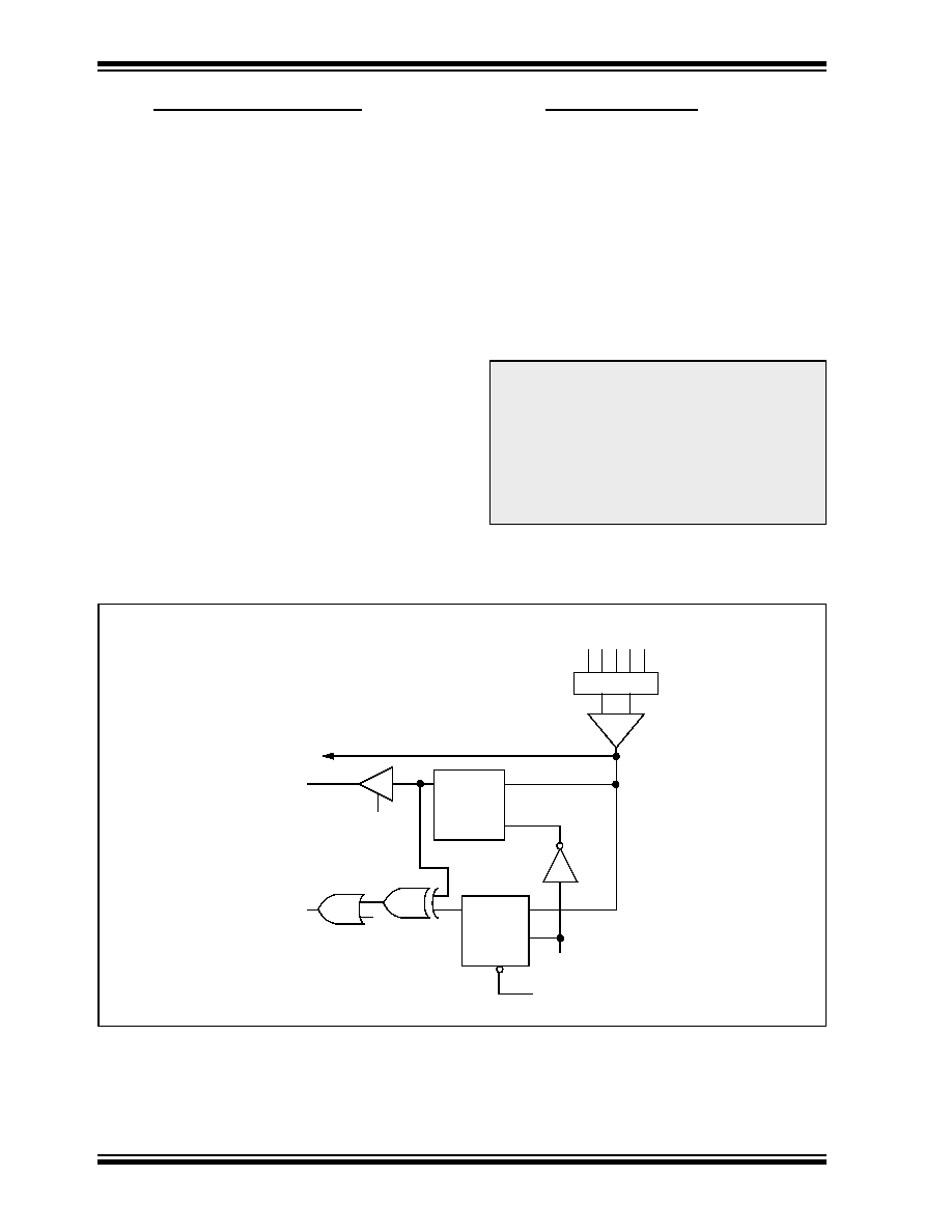
Comparator Outputs
The comparator outputs are read through the CMCON
register. These bits are read only. The comparator
outputs may also be directly output to the RA3 and RA4
I/O pins. When the CM<2:0> = 110, multiplexors in the
output path of the RA3 and RA4 pins will switch and the
output of each pin will be the unsynchronized output of
the comparator. The uncertainty of each of the
comparators is related to the input offset voltage and
the
response
time
given
in
the
specifications.
Figure 8-3 shows the comparator output block diagram.
The TRISA bits will still function as an output
enable/disable for the RA3 and RA4 pins while in this
mode.
Note 1: When reading the PORT register, all pins
configured as analog inputs will read as
a ‘0’. Pins configured as digital inputs will
convert an analog input according to the
Schmitt Trigger input specification.
2: Analog levels on any pin that is defined
as a digital input may cause the input
buffer to consume more current than is
specified.
FIGURE 8-3:
COMPARATOR OUTPUT BLOCK DIAGRAM
D
Q
EN
To RA3 or
RA4 Pin
Data
Bus
RD CMCON
Set
MULTIPLEX
CMIF
Bit
-
+
Q
CL
Port Pins
RD CMCON
NRESET
From
Other
Comparator
EN
D
相关PDF资料 |
PDF描述 |
|---|---|
| PIC16F916-I/SO | IC PIC MCU FLASH 8KX14 28SOIC |
| PIC18F1220-I/SO | IC MCU FLASH 2KX16 A/D 18SOIC |
| PIC18F1220-I/SS | IC MCU FLASH 2KX16 A/D 20SSOP |
| HFW5S-2STE1 | HFW5S-2STE1-HFW5S-2STE1 |
| PIC18F2221-I/SO | IC PIC MCU FLASH 2KX16 28SOIC |
相关代理商/技术参数 |
参数描述 |
|---|---|
| PIC16CE625-20/P | 功能描述:8位微控制器 -MCU 3.5KB 128 RAM 13 I/O RoHS:否 制造商:Silicon Labs 核心:8051 处理器系列:C8051F39x 数据总线宽度:8 bit 最大时钟频率:50 MHz 程序存储器大小:16 KB 数据 RAM 大小:1 KB 片上 ADC:Yes 工作电源电压:1.8 V to 3.6 V 工作温度范围:- 40 C to + 105 C 封装 / 箱体:QFN-20 安装风格:SMD/SMT |
| PIC16CE625-20/SO | 功能描述:8位微控制器 -MCU 3.5KB 128 RAM 13 I/O RoHS:否 制造商:Silicon Labs 核心:8051 处理器系列:C8051F39x 数据总线宽度:8 bit 最大时钟频率:50 MHz 程序存储器大小:16 KB 数据 RAM 大小:1 KB 片上 ADC:Yes 工作电源电压:1.8 V to 3.6 V 工作温度范围:- 40 C to + 105 C 封装 / 箱体:QFN-20 安装风格:SMD/SMT |
| PIC16CE625-20/SS | 功能描述:8位微控制器 -MCU 3.5KB 128 RAM 13 I/O RoHS:否 制造商:Silicon Labs 核心:8051 处理器系列:C8051F39x 数据总线宽度:8 bit 最大时钟频率:50 MHz 程序存储器大小:16 KB 数据 RAM 大小:1 KB 片上 ADC:Yes 工作电源电压:1.8 V to 3.6 V 工作温度范围:- 40 C to + 105 C 封装 / 箱体:QFN-20 安装风格:SMD/SMT |
| PIC16CE625-20E/P | 功能描述:8位微控制器 -MCU 3.5KB 128 RAM 13 I/O RoHS:否 制造商:Silicon Labs 核心:8051 处理器系列:C8051F39x 数据总线宽度:8 bit 最大时钟频率:50 MHz 程序存储器大小:16 KB 数据 RAM 大小:1 KB 片上 ADC:Yes 工作电源电压:1.8 V to 3.6 V 工作温度范围:- 40 C to + 105 C 封装 / 箱体:QFN-20 安装风格:SMD/SMT |
| PIC16CE625-20E/SO | 功能描述:8位微控制器 -MCU 3.5KB 128 RAM 13 I/O RoHS:否 制造商:Silicon Labs 核心:8051 处理器系列:C8051F39x 数据总线宽度:8 bit 最大时钟频率:50 MHz 程序存储器大小:16 KB 数据 RAM 大小:1 KB 片上 ADC:Yes 工作电源电压:1.8 V to 3.6 V 工作温度范围:- 40 C to + 105 C 封装 / 箱体:QFN-20 安装风格:SMD/SMT |
发布紧急采购,3分钟左右您将得到回复。