- 您现在的位置:买卖IC网 > PDF目录11604 > PIC16F1512-E/MV (Microchip Technology)IC MCU 8BIT 3.5KB FLASH 28-UQFN PDF资料下载
参数资料
| 型号: | PIC16F1512-E/MV |
| 厂商: | Microchip Technology |
| 文件页数: | 132/348页 |
| 文件大小: | 0K |
| 描述: | IC MCU 8BIT 3.5KB FLASH 28-UQFN |
| 标准包装: | 91 |
| 系列: | PIC® XLP™ 16F |
| 核心处理器: | PIC |
| 芯体尺寸: | 8-位 |
| 速度: | 20MHz |
| 连通性: | I²C,LIN,SPI,UART/USART |
| 外围设备: | 欠压检测/复位,POR,PWM,WDT |
| 输入/输出数: | 25 |
| 程序存储器容量: | 3.5KB(2K x 14) |
| 程序存储器类型: | 闪存 |
| RAM 容量: | 128 x 8 |
| 电压 - 电源 (Vcc/Vdd): | 2.3 V ~ 5.5 V |
| 数据转换器: | A/D 17x10b |
| 振荡器型: | 内部 |
| 工作温度: | -40°C ~ 125°C |
| 封装/外壳: | 28-UFQFN 裸露焊盘 |
| 包装: | 管件 |
第1页第2页第3页第4页第5页第6页第7页第8页第9页第10页第11页第12页第13页第14页第15页第16页第17页第18页第19页第20页第21页第22页第23页第24页第25页第26页第27页第28页第29页第30页第31页第32页第33页第34页第35页第36页第37页第38页第39页第40页第41页第42页第43页第44页第45页第46页第47页第48页第49页第50页第51页第52页第53页第54页第55页第56页第57页第58页第59页第60页第61页第62页第63页第64页第65页第66页第67页第68页第69页第70页第71页第72页第73页第74页第75页第76页第77页第78页第79页第80页第81页第82页第83页第84页第85页第86页第87页第88页第89页第90页第91页第92页第93页第94页第95页第96页第97页第98页第99页第100页第101页第102页第103页第104页第105页第106页第107页第108页第109页第110页第111页第112页第113页第114页第115页第116页第117页第118页第119页第120页第121页第122页第123页第124页第125页第126页第127页第128页第129页第130页第131页当前第132页第133页第134页第135页第136页第137页第138页第139页第140页第141页第142页第143页第144页第145页第146页第147页第148页第149页第150页第151页第152页第153页第154页第155页第156页第157页第158页第159页第160页第161页第162页第163页第164页第165页第166页第167页第168页第169页第170页第171页第172页第173页第174页第175页第176页第177页第178页第179页第180页第181页第182页第183页第184页第185页第186页第187页第188页第189页第190页第191页第192页第193页第194页第195页第196页第197页第198页第199页第200页第201页第202页第203页第204页第205页第206页第207页第208页第209页第210页第211页第212页第213页第214页第215页第216页第217页第218页第219页第220页第221页第222页第223页第224页第225页第226页第227页第228页第229页第230页第231页第232页第233页第234页第235页第236页第237页第238页第239页第240页第241页第242页第243页第244页第245页第246页第247页第248页第249页第250页第251页第252页第253页第254页第255页第256页第257页第258页第259页第260页第261页第262页第263页第264页第265页第266页第267页第268页第269页第270页第271页第272页第273页第274页第275页第276页第277页第278页第279页第280页第281页第282页第283页第284页第285页第286页第287页第288页第289页第290页第291页第292页第293页第294页第295页第296页第297页第298页第299页第300页第301页第302页第303页第304页第305页第306页第307页第308页第309页第310页第311页第312页第313页第314页第315页第316页第317页第318页第319页第320页第321页第322页第323页第324页第325页第326页第327页第328页第329页第330页第331页第332页第333页第334页第335页第336页第337页第338页第339页第340页第341页第342页第343页第344页第345页第346页第347页第348页
2012 Microchip Technology Inc.
Preliminary
DS41624B-page 217
PIC16(L)F1512/3
20.6.5
I2C MASTER MODE REPEATED
START CONDITION TIMING
A Repeated Start condition occurs when the RSEN bit
of the SSPCON2 register is programmed high and the
Master state machine is no longer active. When the
RSEN bit is set, the SCL pin is asserted low. When the
SCL pin is sampled low, the Baud Rate Generator is
loaded and begins counting. The SDA pin is released
(brought high) for one Baud Rate Generator count
(TBRG). When the Baud Rate Generator times out, if
SDA is sampled high, the SCL pin will be deasserted
(brought high). When SCL is sampled high, the Baud
Rate Generator is reloaded and begins counting. SDA
and SCL must be sampled high for one TBRG. This
action is then followed by assertion of the SDA pin
(SDA = 0) for one TBRG while SCL is high. SCL is
asserted low. Following this, the RSEN bit of the
SSPCON2 register will be automatically cleared and
the Baud Rate Generator will not be reloaded, leaving
the SDA pin held low. As soon as a Start condition is
detected on the SDA and SCL pins, the S bit of the
SSPSTAT register will be set. The SSPIF bit will not be
set until the Baud Rate Generator has timed out.
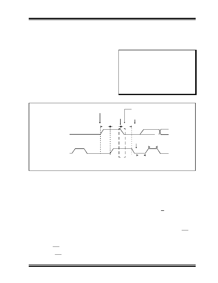
FIGURE 20-27:
REPEAT START CONDITION WAVEFORM
20.6.6
I2C MASTER MODE
TRANSMISSION
Transmission of a data byte, a 7-bit address or the
other half of a 10-bit address is accomplished by simply
writing a value to the SSPBUF register. This action will
set the Buffer Full flag bit, BF and allow the Baud Rate
Generator to begin counting and start the next trans-
mission. Each bit of address/data will be shifted out
onto the SDA pin after the falling edge of SCL is
asserted. SCL is held low for one Baud Rate Generator
rollover count (TBRG). Data should be valid before SCL
is released high. When the SCL pin is released high, it
is held that way for TBRG. The data on the SDA pin
must remain stable for that duration and some hold
time after the next falling edge of SCL. After the eighth
bit is shifted out (the falling edge of the eighth clock),
the BF flag is cleared and the master releases SDA.
This allows the slave device being addressed to
respond with an ACK bit during the ninth bit time if an
address match occurred, or if data was received prop-
erly. The status of ACK is written into the ACKSTAT bit
on the rising edge of the ninth clock. If the master
receives an Acknowledge, the Acknowledge Status bit,
ACKSTAT, is cleared. If not, the bit is set. After the ninth
clock, the SSPIF bit is set and the master clock (Baud
Rate Generator) is suspended until the next data byte
is loaded into the SSPBUF, leaving SCL low and SDA
unchanged (Figure 20-27).
After the write to the SSPBUF, each bit of the address
will be shifted out on the falling edge of SCL until all
seven address bits and the R/W bit are completed. On
the falling edge of the eighth clock, the master will
release the SDA pin, allowing the slave to respond with
an Acknowledge. On the falling edge of the ninth clock,
the master will sample the SDA pin to see if the address
was recognized by a slave. The status of the ACK bit is
loaded into the ACKSTAT Status bit of the SSPCON2
register. Following the falling edge of the ninth clock
transmission of the address, the SSPIF is set, the BF
flag is cleared and the Baud Rate Generator is turned
off until another write to the SSPBUF takes place,
holding SCL low and allowing SDA to float.
Note 1:
If RSEN is programmed while any other
event is in progress, it will not take effect.
2:
A bus collision during the Repeated Start
condition occurs if:
SDA is sampled low when SCL
goes from low-to-high.
SCL goes low before SDA is
asserted low. This may indicate
that another master is attempting to
transmit a data ‘1’.
SDA
SCL
Repeated Start
Write to SSPCON2
Write to SSPBUF occurs here
At completion of Start bit,
hardware clears RSEN bit
1st bit
S bit set by hardware
TBRG
SDA = 1,
SCL (no change)
SCL = 1
occurs here
TBRG
and sets SSPIF
Sr
相关PDF资料 |
PDF描述 |
|---|---|
| MS27467T25B46S | CONN PLUG 46POS STRAIGHT W/SCKT |
| PIC16LF1825T-I/SL | MCU PIC 14KB FLASH 14-SOIC |
| D38999/20MJ24SN | CONN RCPT 24POS WALL MNT W/SCKT |
| PIC16F1825T-I/SL | MCU PIC 14K FLASH 1K RAM 14SOIC |
| PIC16F1824T-I/ST | IC MCU 8BIT 7KB FLASH 14TSSOP |
相关代理商/技术参数 |
参数描述 |
|---|---|
| PIC16F1512-I/MV | 功能描述:8位微控制器 -MCU 3.5KB Flash 128B RAM 10-bit ADC RoHS:否 制造商:Silicon Labs 核心:8051 处理器系列:C8051F39x 数据总线宽度:8 bit 最大时钟频率:50 MHz 程序存储器大小:16 KB 数据 RAM 大小:1 KB 片上 ADC:Yes 工作电源电压:1.8 V to 3.6 V 工作温度范围:- 40 C to + 105 C 封装 / 箱体:QFN-20 安装风格:SMD/SMT |
| PIC16F1512-I/SO | 功能描述:8位微控制器 -MCU 3.5KB Flash 128B RAM 10-bit ADC RoHS:否 制造商:Silicon Labs 核心:8051 处理器系列:C8051F39x 数据总线宽度:8 bit 最大时钟频率:50 MHz 程序存储器大小:16 KB 数据 RAM 大小:1 KB 片上 ADC:Yes 工作电源电压:1.8 V to 3.6 V 工作温度范围:- 40 C to + 105 C 封装 / 箱体:QFN-20 安装风格:SMD/SMT |
| PIC16F1512-I/SP | 功能描述:8位微控制器 -MCU 3.5KB Flash 128B RAM 10-bit ADC RoHS:否 制造商:Silicon Labs 核心:8051 处理器系列:C8051F39x 数据总线宽度:8 bit 最大时钟频率:50 MHz 程序存储器大小:16 KB 数据 RAM 大小:1 KB 片上 ADC:Yes 工作电源电压:1.8 V to 3.6 V 工作温度范围:- 40 C to + 105 C 封装 / 箱体:QFN-20 安装风格:SMD/SMT |
| PIC16F1512-I/SS | 功能描述:8位微控制器 -MCU 3.5KB Flash 128B RAM 10-bit ADC RoHS:否 制造商:Silicon Labs 核心:8051 处理器系列:C8051F39x 数据总线宽度:8 bit 最大时钟频率:50 MHz 程序存储器大小:16 KB 数据 RAM 大小:1 KB 片上 ADC:Yes 工作电源电压:1.8 V to 3.6 V 工作温度范围:- 40 C to + 105 C 封装 / 箱体:QFN-20 安装风格:SMD/SMT |
| PIC16F1512T-I/MV | 功能描述:8位微控制器 -MCU 3.5KB Flash 128B RAM 10-bit ADC RoHS:否 制造商:Silicon Labs 核心:8051 处理器系列:C8051F39x 数据总线宽度:8 bit 最大时钟频率:50 MHz 程序存储器大小:16 KB 数据 RAM 大小:1 KB 片上 ADC:Yes 工作电源电压:1.8 V to 3.6 V 工作温度范围:- 40 C to + 105 C 封装 / 箱体:QFN-20 安装风格:SMD/SMT |
发布紧急采购,3分钟左右您将得到回复。