参数资料
| 型号: | PIC16F1939-I/P |
| 厂商: | Microchip Technology |
| 文件页数: | 19/92页 |
| 文件大小: | 0K |
| 描述: | IC MCU 8BIT FLASH 40-DIP |
| 产品培训模块: | 8-bit PIC® Microcontroller Portfolio |
| 特色产品: | Extreme Low Power (XLP) Microcontrollers |
| 标准包装: | 10 |
| 系列: | PIC® XLP™ 16F |
| 核心处理器: | PIC |
| 芯体尺寸: | 8-位 |
| 速度: | 32MHz |
| 连通性: | I²C,LIN,SPI,UART/USART |
| 外围设备: | 欠压检测/复位,LCD,POR,PWM,WDT |
| 输入/输出数: | 36 |
| 程序存储器容量: | 28KB(16K x 14) |
| 程序存储器类型: | 闪存 |
| EEPROM 大小: | 256 x 8 |
| RAM 容量: | 1K x 8 |
| 电压 - 电源 (Vcc/Vdd): | 1.8 V ~ 5.5 V |
| 数据转换器: | A/D 14x10b |
| 振荡器型: | 内部 |
| 工作温度: | -40°C ~ 85°C |
| 封装/外壳: | 40-DIP(0.600",15.24mm) |
| 包装: | 管件 |
第1页第2页第3页第4页第5页第6页第7页第8页第9页第10页第11页第12页第13页第14页第15页第16页第17页第18页当前第19页第20页第21页第22页第23页第24页第25页第26页第27页第28页第29页第30页第31页第32页第33页第34页第35页第36页第37页第38页第39页第40页第41页第42页第43页第44页第45页第46页第47页第48页第49页第50页第51页第52页第53页第54页第55页第56页第57页第58页第59页第60页第61页第62页第63页第64页第65页第66页第67页第68页第69页第70页第71页第72页第73页第74页第75页第76页第77页第78页第79页第80页第81页第82页第83页第84页第85页第86页第87页第88页第89页第90页第91页第92页
2009 Microchip Technology Inc.
DS39637D-page 135
PIC18F2480/2580/4480/4580
11.0 I/O PORTS
Depending on the device selected and features
enabled, there are up to five ports available. Some pins
of the I/O ports are multiplexed with an alternate
function from the peripheral features on the device. In
general, when a peripheral is enabled, that pin may not
be used as a general purpose I/O pin.
Each port has three registers for its operation. These
registers are:
TRIS register (Data Direction register)
PORT register (reads the levels on the pins of the
device)
LAT register (Output Latch register)
The Output Latch register (LAT) is useful for read-
modify-write operations on the value that the I/O pins
are driving.
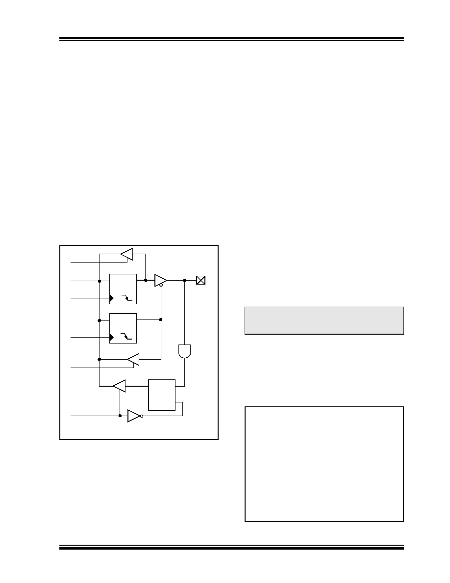
A simplified model of a generic I/O port, without the
interfaces to other peripherals, is shown in Figure 11-1.
FIGURE 11-1:
GENERIC I/O PORT
OPERATION
11.1
PORTA, TRISA and LATA Registers
PORTA is an 8-bit wide, bidirectional port. The
corresponding Data Direction register is TRISA. Setting
a TRISA bit (= 1) will make the corresponding PORTA
pin an input (i.e., put the corresponding output driver in
a high-impedance mode). Clearing a TRISA bit (= 0)
will make the corresponding PORTA pin an output (i.e.,
put the contents of the Output Latch register on the
selected pin).
Reading the PORTA register reads the status of the
pins, whereas writing to it, will write to the port latch.
The Output Latch register (LATA) is also memory
mapped. Read-modify-write operations on the LATA
register read and write the latched output value for
PORTA.
The RA4 pin is multiplexed with the Timer0 module
clock input to become the RA4/T0CKI pin. Pins, RA6
and RA7, are multiplexed with the main oscillator pins;
they are enabled as oscillator or I/O pins by the selec-
tion of the main oscillator in Configuration Register 1H
(see Section 25.1 “Configuration Bits” for details).
When they are not used as port pins, RA6 and RA7 and
their associated TRIS and LAT bits are read as ‘0’.
The other PORTA pins are multiplexed with analog
inputs, the analog VREF+ and VREF- inputs and the
comparator voltage reference output. The operation of
pins, RA<3:0> and RA5 as A/D Converter inputs, is
selected by clearing/setting the control bits in the
ADCON1 register (A/D Control Register 1).
All other PORTA pins have TTL input levels and full
CMOS output drivers.
The TRISA register controls the direction of the RA
pins, even when they are being used as analog inputs.
The user must ensure the bits in the TRISA register are
maintained set when using them as analog inputs.
EXAMPLE 11-1:
INITIALIZING PORTA
Data
Bus
WR LAT
WR TRIS
RD PORT
Data Latch
TRIS Latch
RD TRIS
Input
Buffer
I/O pin(1)
Q
D
CK
Q
D
CK
EN
QD
EN
RD LAT
or PORT
Note 1:
I/O pins have diode protection to VDD and VSS.
Note:
On a Power-on Reset, RA5 and RA<3:0>
are configured as analog inputs and read
as ‘0’. RA4 is configured as a digital input.
CLRF
PORTA
; Initialize PORTA by
; clearing output
; data latches
CLRF
LATA
; Alternate method
; to clear output
; data latches
MOVLW
0Fh
; Configure A/D
MOVWF
ADCON1 ; for digital inputs
MOVWF
07h
; Configure comparators
MOVWF
CMCON
; for digital input
MOVLW
0CFh
; Value used to
; initialize data
; direction
MOVWF
TRISA
; Set RA<3:0> as inputs
; RA<5:4> as outputs
相关PDF资料 |
PDF描述 |
|---|---|
| PIC24FJ128GB110T-I/PF | IC PIC MCU FLASH 100TQFP |
| PIC24FJ128GA110T-I/PT | IC PIC MCU FLASH 100TQFP |
| PIC18F44K22-I/PT | IC PIC MCU 16KB FLASH 44TQFP |
| PIC24FJ128GA110T-I/PF | IC PIC MCU FLASH 100TQFP |
| PIC18LF8393-I/PT | IC PIC MCU FLASH 4KX16 80TQFP |
相关代理商/技术参数 |
参数描述 |
|---|---|
| PIC16F1939T-I/ML | 功能描述:8位微控制器 -MCU 28KB Flash 1.8-5.5V 1KB RAM 256B EEPROM RoHS:否 制造商:Silicon Labs 核心:8051 处理器系列:C8051F39x 数据总线宽度:8 bit 最大时钟频率:50 MHz 程序存储器大小:16 KB 数据 RAM 大小:1 KB 片上 ADC:Yes 工作电源电压:1.8 V to 3.6 V 工作温度范围:- 40 C to + 105 C 封装 / 箱体:QFN-20 安装风格:SMD/SMT |
| PIC16F1939T-I/MV | 功能描述:8位微控制器 -MCU 28KB Fl 1KB R 256B 1.8-5.5V RoHS:否 制造商:Silicon Labs 核心:8051 处理器系列:C8051F39x 数据总线宽度:8 bit 最大时钟频率:50 MHz 程序存储器大小:16 KB 数据 RAM 大小:1 KB 片上 ADC:Yes 工作电源电压:1.8 V to 3.6 V 工作温度范围:- 40 C to + 105 C 封装 / 箱体:QFN-20 安装风格:SMD/SMT |
| PIC16F1939T-I/PT | 功能描述:8位微控制器 -MCU 28KB Flash 1.8-5.5V 1KB RAM 256B EEPROM RoHS:否 制造商:Silicon Labs 核心:8051 处理器系列:C8051F39x 数据总线宽度:8 bit 最大时钟频率:50 MHz 程序存储器大小:16 KB 数据 RAM 大小:1 KB 片上 ADC:Yes 工作电源电压:1.8 V to 3.6 V 工作温度范围:- 40 C to + 105 C 封装 / 箱体:QFN-20 安装风格:SMD/SMT |
| PIC16F1946-E/MR | 功能描述:8位微控制器 -MCU 14KB 512B RM 256B EEPROM LCD 1.8-5.5V RoHS:否 制造商:Silicon Labs 核心:8051 处理器系列:C8051F39x 数据总线宽度:8 bit 最大时钟频率:50 MHz 程序存储器大小:16 KB 数据 RAM 大小:1 KB 片上 ADC:Yes 工作电源电压:1.8 V to 3.6 V 工作温度范围:- 40 C to + 105 C 封装 / 箱体:QFN-20 安装风格:SMD/SMT |
| PIC16F1946-E/PT | 功能描述:8位微控制器 -MCU 14KB Flash, 512B RAM LCD, 1.8-5.5V RoHS:否 制造商:Silicon Labs 核心:8051 处理器系列:C8051F39x 数据总线宽度:8 bit 最大时钟频率:50 MHz 程序存储器大小:16 KB 数据 RAM 大小:1 KB 片上 ADC:Yes 工作电源电压:1.8 V to 3.6 V 工作温度范围:- 40 C to + 105 C 封装 / 箱体:QFN-20 安装风格:SMD/SMT |
发布紧急采购,3分钟左右您将得到回复。