- 您现在的位置:买卖IC网 > PDF目录11476 > PIC16F628T-20/SS (Microchip Technology)IC MCU FLASH 2KX14 COMP 20SSOP PDF资料下载
参数资料
| 型号: | PIC16F628T-20/SS |
| 厂商: | Microchip Technology |
| 文件页数: | 18/180页 |
| 文件大小: | 0K |
| 描述: | IC MCU FLASH 2KX14 COMP 20SSOP |
| 产品培训模块: | Asynchronous Stimulus |
| 标准包装: | 1,600 |
| 系列: | PIC® 16F |
| 核心处理器: | PIC |
| 芯体尺寸: | 8-位 |
| 速度: | 20MHz |
| 连通性: | UART/USART |
| 外围设备: | 欠压检测/复位,POR,PWM,WDT |
| 输入/输出数: | 16 |
| 程序存储器容量: | 3.5KB(2K x 14) |
| 程序存储器类型: | 闪存 |
| EEPROM 大小: | 128 x 8 |
| RAM 容量: | 224 x 8 |
| 电压 - 电源 (Vcc/Vdd): | 3 V ~ 5.5 V |
| 振荡器型: | 内部 |
| 工作温度: | 0°C ~ 70°C |
| 封装/外壳: | 20-SSOP(0.209",5.30mm 宽) |
| 包装: | 带卷 (TR) |
第1页第2页第3页第4页第5页第6页第7页第8页第9页第10页第11页第12页第13页第14页第15页第16页第17页当前第18页第19页第20页第21页第22页第23页第24页第25页第26页第27页第28页第29页第30页第31页第32页第33页第34页第35页第36页第37页第38页第39页第40页第41页第42页第43页第44页第45页第46页第47页第48页第49页第50页第51页第52页第53页第54页第55页第56页第57页第58页第59页第60页第61页第62页第63页第64页第65页第66页第67页第68页第69页第70页第71页第72页第73页第74页第75页第76页第77页第78页第79页第80页第81页第82页第83页第84页第85页第86页第87页第88页第89页第90页第91页第92页第93页第94页第95页第96页第97页第98页第99页第100页第101页第102页第103页第104页第105页第106页第107页第108页第109页第110页第111页第112页第113页第114页第115页第116页第117页第118页第119页第120页第121页第122页第123页第124页第125页第126页第127页第128页第129页第130页第131页第132页第133页第134页第135页第136页第137页第138页第139页第140页第141页第142页第143页第144页第145页第146页第147页第148页第149页第150页第151页第152页第153页第154页第155页第156页第157页第158页第159页第160页第161页第162页第163页第164页第165页第166页第167页第168页第169页第170页第171页第172页第173页第174页第175页第176页第177页第178页第179页第180页
PIC16F627A/628A/648A
DS40044G-page 114
2009 Microchip Technology Inc.
14.11 In-Circuit Serial Programming
(ICSP)
The PIC16F627A/628A/648A microcontrollers can be
serially programmed while in the end application circuit.
This is simply done with two lines for clock and data,
and three other lines for power, ground and the
programming voltage. This allows customers to
manufacture boards with unprogrammed devices and
then program the microcontroller just before shipping
the product. This also allows the most recent firmware
or custom firmware to be programmed.
The device is placed into a Program/Verify mode by
holding the RB6 and RB7 pins low while raising the
MCLR (VPP) pin from VIL to VIHH. See “PIC16F627A/
628A/648A
EEPROM
Memory
Programming
Specification
” (DS41196) for details. RB6 becomes the
programming clock and RB7 becomes the programming
data. Both RB6 and RB7 are Schmitt Trigger inputs in
this mode.
After Reset, to place the device into Programming/Verify
mode, the Program Counter (PC) is at location 00h. A
6-bit command is then supplied to the device. Depending
on the command, 14 bits of program data are then
supplied to or from the device, depending if the command
was a load or a read. For complete details of serial
programming, please refer to “PIC16F627A/628A/648A
EEPROM
Memory
Programming
Specification
”
(DS41196).
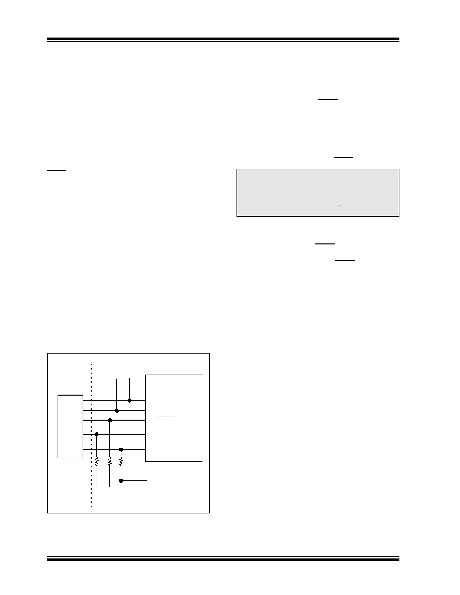
A typical In-Circuit Serial Programming connection is
shown in Figure 14-18.
FIGURE 14-18:
TYPICAL IN-CIRCUIT
SERIAL PROGRAMMING
CONNECTION
14.12 Low-Voltage Programming
The LVP bit of the Configuration Word, enables the low-
voltage
programming.
This
mode
allows
the
microcontroller to be programmed via ICSP using only
a 5V source. This mode removes the requirement of
VIHH to be placed on the MCLR pin. The LVP bit is
normally erased to ‘1’ which enables the low-voltage
programming. In this mode, the RB4/PGM pin is
dedicated to the programming function and ceases to
be a general purpose I/O pin. The device will enter
Programming mode when a ‘1’ is placed on the RB4/
PGM pin. The High-Voltage Programming mode is still
available by placing VIHH on the MCLR pin.
If Low-Voltage Programming mode is not used, the
LVP bit should be programmed to a ‘0’ so that RB4/
PGM becomes a digital I/O pin. To program the device,
VIHH must be placed onto MCLR during programming.
The LVP bit may only be programmed when program-
ming is entered with VIHH on MCLR. The LVP bit
cannot be programmed when programming is entered
with RB4/PGM.
It should be noted, that once the LVP bit is programmed
to ‘0’, only High-Voltage Programming mode can be
used to program the device.
External
Connector
Signals
To Normal
Connections
To Normal
Connections
PIC16F627A/628A/648A
VDD
VSS
RA5/MCLR/VPP
RB6/PGC
RB7/PGD
+5V
0V
VPP
CLK
Data I/O
VDD
Note 1:
While in this mode, the RB4 pin can no
longer be used as a general purpose I/O
pin.
2:
VDD must be 5.0V +10% during erase
operations.
相关PDF资料 |
PDF描述 |
|---|---|
| PIC16LCE623-04/SO | IC MCU OTP 512X14 EE 18SOIC |
| PIC16CE625-04/SS | IC MCU OTP 2KX14 EE COMP 20SSOP |
| PIC16C711T-04E/SO | IC MCU OTP 1KX14 A/D 18SOIC |
| PIC16C54-XT/SS | IC MCU OTP 512X12 20SSOP |
| PIC16C54-RC/SS | IC MCU OTP 512X12 20SSOP |
相关代理商/技术参数 |
参数描述 |
|---|---|
| PIC16F630-E/ML | 功能描述:8位微控制器 -MCU 1.75KB 64 RAM 12I/O Ext Temp QFN RoHS:否 制造商:Silicon Labs 核心:8051 处理器系列:C8051F39x 数据总线宽度:8 bit 最大时钟频率:50 MHz 程序存储器大小:16 KB 数据 RAM 大小:1 KB 片上 ADC:Yes 工作电源电压:1.8 V to 3.6 V 工作温度范围:- 40 C to + 105 C 封装 / 箱体:QFN-20 安装风格:SMD/SMT |
| PIC16F630-E/P | 功能描述:8位微控制器 -MCU 1.75KB 64 RAM 12 I/O Ext Temp PDIP14 RoHS:否 制造商:Silicon Labs 核心:8051 处理器系列:C8051F39x 数据总线宽度:8 bit 最大时钟频率:50 MHz 程序存储器大小:16 KB 数据 RAM 大小:1 KB 片上 ADC:Yes 工作电源电压:1.8 V to 3.6 V 工作温度范围:- 40 C to + 105 C 封装 / 箱体:QFN-20 安装风格:SMD/SMT |
| PIC16F630-E/SL | 功能描述:8位微控制器 -MCU 1.75KB 64 RAM 12 I/O Ext Temp SOIC14 RoHS:否 制造商:Silicon Labs 核心:8051 处理器系列:C8051F39x 数据总线宽度:8 bit 最大时钟频率:50 MHz 程序存储器大小:16 KB 数据 RAM 大小:1 KB 片上 ADC:Yes 工作电源电压:1.8 V to 3.6 V 工作温度范围:- 40 C to + 105 C 封装 / 箱体:QFN-20 安装风格:SMD/SMT |
| PIC16F630-E/ST | 功能描述:8位微控制器 -MCU 1.75KB 64 RAM 12 I/O Ext Temp TSSOP14 RoHS:否 制造商:Silicon Labs 核心:8051 处理器系列:C8051F39x 数据总线宽度:8 bit 最大时钟频率:50 MHz 程序存储器大小:16 KB 数据 RAM 大小:1 KB 片上 ADC:Yes 工作电源电压:1.8 V to 3.6 V 工作温度范围:- 40 C to + 105 C 封装 / 箱体:QFN-20 安装风格:SMD/SMT |
| PIC16F630-I/ML | 功能描述:8位微控制器 -MCU 1.75KB 64 RAM 12I/O Ind Temp QFN RoHS:否 制造商:Silicon Labs 核心:8051 处理器系列:C8051F39x 数据总线宽度:8 bit 最大时钟频率:50 MHz 程序存储器大小:16 KB 数据 RAM 大小:1 KB 片上 ADC:Yes 工作电源电压:1.8 V to 3.6 V 工作温度范围:- 40 C to + 105 C 封装 / 箱体:QFN-20 安装风格:SMD/SMT |
发布紧急采购,3分钟左右您将得到回复。