- 您现在的位置:买卖IC网 > PDF目录11530 > PIC16F648AT-E/SS (Microchip Technology)IC MCU FLASH 4KX14 EEPROM 20SSOP PDF资料下载
参数资料
| 型号: | PIC16F648AT-E/SS |
| 厂商: | Microchip Technology |
| 文件页数: | 105/180页 |
| 文件大小: | 0K |
| 描述: | IC MCU FLASH 4KX14 EEPROM 20SSOP |
| 产品培训模块: | Asynchronous Stimulus |
| 标准包装: | 1,600 |
| 系列: | PIC® 16F |
| 核心处理器: | PIC |
| 芯体尺寸: | 8-位 |
| 速度: | 20MHz |
| 连通性: | UART/USART |
| 外围设备: | 欠压检测/复位,POR,PWM,WDT |
| 输入/输出数: | 16 |
| 程序存储器容量: | 7KB(4K x 14) |
| 程序存储器类型: | 闪存 |
| EEPROM 大小: | 256 x 8 |
| RAM 容量: | 256 x 8 |
| 电压 - 电源 (Vcc/Vdd): | 3 V ~ 5.5 V |
| 振荡器型: | 内部 |
| 工作温度: | -40°C ~ 125°C |
| 封装/外壳: | 20-SSOP(0.209",5.30mm 宽) |
| 包装: | 带卷 (TR) |
| 配用: | I3DBF648-ND - BOARD DAUGHTER ICEPIC3 |
第1页第2页第3页第4页第5页第6页第7页第8页第9页第10页第11页第12页第13页第14页第15页第16页第17页第18页第19页第20页第21页第22页第23页第24页第25页第26页第27页第28页第29页第30页第31页第32页第33页第34页第35页第36页第37页第38页第39页第40页第41页第42页第43页第44页第45页第46页第47页第48页第49页第50页第51页第52页第53页第54页第55页第56页第57页第58页第59页第60页第61页第62页第63页第64页第65页第66页第67页第68页第69页第70页第71页第72页第73页第74页第75页第76页第77页第78页第79页第80页第81页第82页第83页第84页第85页第86页第87页第88页第89页第90页第91页第92页第93页第94页第95页第96页第97页第98页第99页第100页第101页第102页第103页第104页当前第105页第106页第107页第108页第109页第110页第111页第112页第113页第114页第115页第116页第117页第118页第119页第120页第121页第122页第123页第124页第125页第126页第127页第128页第129页第130页第131页第132页第133页第134页第135页第136页第137页第138页第139页第140页第141页第142页第143页第144页第145页第146页第147页第148页第149页第150页第151页第152页第153页第154页第155页第156页第157页第158页第159页第160页第161页第162页第163页第164页第165页第166页第167页第168页第169页第170页第171页第172页第173页第174页第175页第176页第177页第178页第179页第180页
PIC16F627A/628A/648A
DS40044G-page 30
2009 Microchip Technology Inc.
4.3
PCL and PCLATH
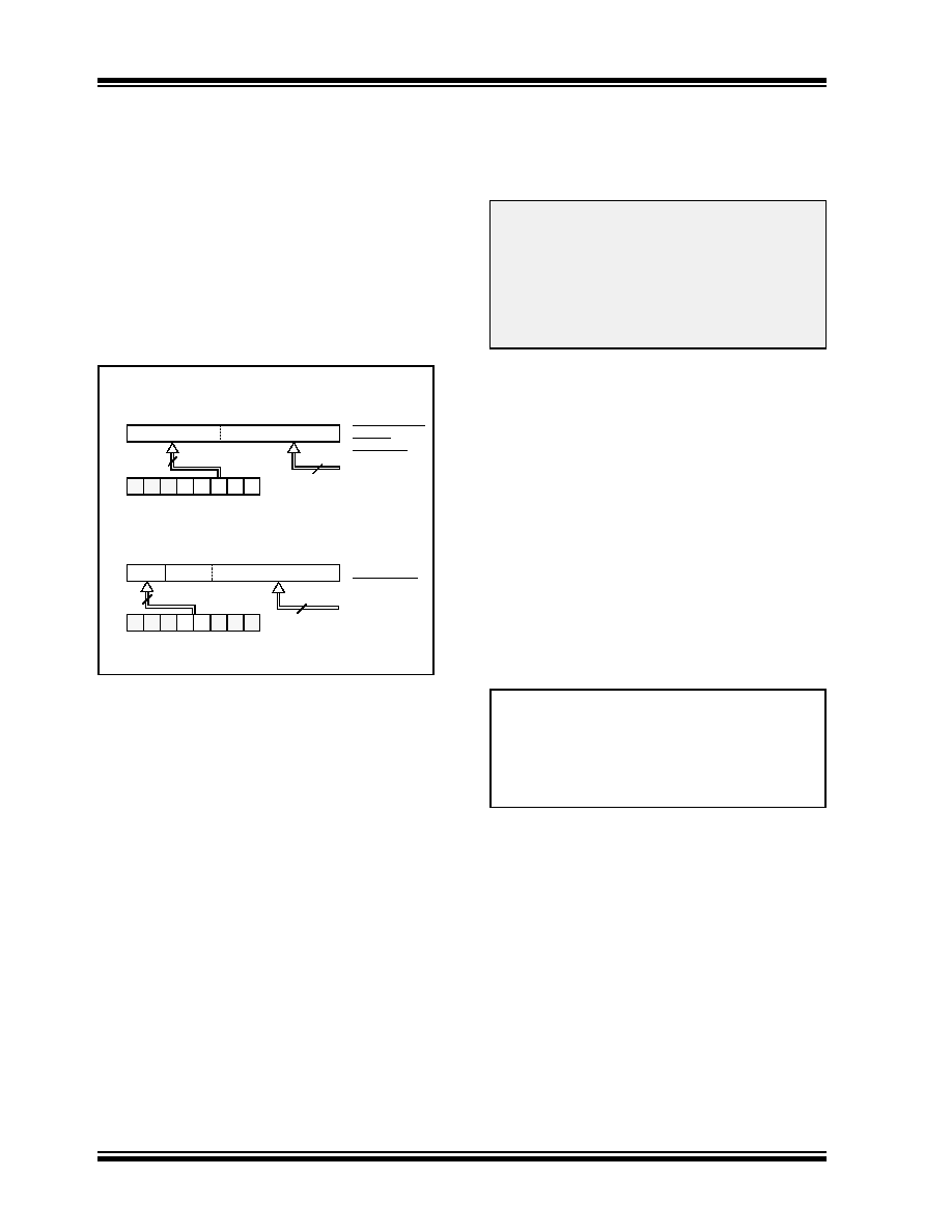
The Program Counter (PC) is 13-bits wide. The low
byte comes from the PCL register, which is a readable
and writable register. The high byte (PC<12:8>) is not
directly readable or writable and comes from PCLATH.
On any Reset, the PC is cleared. Figure 4-4 shows the
two situations for loading the PC. The upper example
in Figure 4-4 shows how the PC is loaded on a write to
PCL (PCLATH<4:0>
→ PCH). The lower example in
Figure 4-4 shows how the PC is loaded during a CALL
or GOTO instruction (PCLATH<4:3>
→ PCH).
FIGURE 4-4:
LOADING OF PC IN
DIFFERENT SITUATIONS
4.3.1
COMPUTED GOTO
A computed GOTO is accomplished by adding an offset
to the program counter (ADDWF PCL). When doing a
table read using a computed GOTO method, care
should be exercised if the table location crosses a PCL
memory boundary (each 256-byte block). Refer to the
Application Note AN556 “Implementing a Table Read”
(DS00556).
4.3.2
STACK
The PIC16F627A/628A/648A family has an 8-level
deep x 13-bit wide hardware stack (Figure 4-1). The
stack space is not part of either program or data space
and the Stack Pointer is not readable or writable. The
PC is PUSHed onto the stack when a CALL instruction
is executed or an interrupt causes a branch. The stack
is POPed in the event of a RETURN, RETLW or a
RETFIE
instruction execution. PCLATH is not affected
by a PUSH or POP operation.
The stack operates as a circular buffer. This means that
after the stack has been PUSHed eight times, the ninth
PUSH overwrites the value that was stored from the
first PUSH. The tenth PUSH overwrites the second
PUSH (and so on).
4.4
Indirect Addressing, INDF and
FSR Registers
The INDF register is not a physical register. Addressing
the INDF register will cause indirect addressing.
Indirect addressing is possible by using the INDF
register. Any instruction using the INDF register
actually accesses data pointed to by the File Select
Register (FSR). Reading INDF itself indirectly will
produce 00h. Writing to the INDF register indirectly
results in a no-operation (although Status bits may be
affected). An effective 9-bit address is obtained by
concatenating the 8-bit FSR register and the IRP bit
(STATUS<7>), as shown in Figure 4-5.
A simple program to clear RAM location 20h-2Fh using
indirect addressing is shown in Example 4-1.
EXAMPLE 4-1:
INDIRECT ADDRESSING
PC
12
8 7
0
5
PCLATH<4:0>
PCLATH
Instruction with
ALU result
GOTO, CALL
Opcode <10:0>
8
PC
12 11 10
0
11
PCLATH<4:3>
PCH
PCL
87
2
PCLATH
PCH
PCL
PCL as
Destination
Note 1:
There are no Status bits to indicate stack
overflow or stack underflow conditions.
2:
There are no instructions/mnemonics
called PUSH or POP. These are actions
that occur from the execution of the
CALL,
RETURN,
RETLW
and RETFIE
instructions, or the vectoring to an
interrupt address.
MOVLW
0x20
;initialize pointer
MOVWF
FSR
;to RAM
NEXT
CLRF
INDF
;clear INDF register
INCF
FSR
;inc pointer
BTFSS
FSR,4
;all done?
GOTO
NEXT
;no clear next
;yes continue
相关PDF资料 |
PDF描述 |
|---|---|
| VE-271-IY-B1 | CONVERTER MOD DC/DC 12V 50W |
| VI-22Z-IW-B1 | CONVERTER MOD DC/DC 2V 40W |
| 000-79700 | CONN ADPT TNC TEE JACK/PLUG/JACK |
| VI-22Y-IY-B1 | CONVERTER MOD DC/DC 3.3V 33W |
| VI-22Y-IX-B1 | CONVERTER MOD DC/DC 3.3V 49.5W |
相关代理商/技术参数 |
参数描述 |
|---|---|
| PIC16F648AT-I/ML | 功能描述:8位微控制器 -MCU 7KB 256 RAM 16 I/O RoHS:否 制造商:Silicon Labs 核心:8051 处理器系列:C8051F39x 数据总线宽度:8 bit 最大时钟频率:50 MHz 程序存储器大小:16 KB 数据 RAM 大小:1 KB 片上 ADC:Yes 工作电源电压:1.8 V to 3.6 V 工作温度范围:- 40 C to + 105 C 封装 / 箱体:QFN-20 安装风格:SMD/SMT |
| PIC16F648AT-I/SO | 功能描述:8位微控制器 -MCU 7KB 256 RAM 16 I/O RoHS:否 制造商:Silicon Labs 核心:8051 处理器系列:C8051F39x 数据总线宽度:8 bit 最大时钟频率:50 MHz 程序存储器大小:16 KB 数据 RAM 大小:1 KB 片上 ADC:Yes 工作电源电压:1.8 V to 3.6 V 工作温度范围:- 40 C to + 105 C 封装 / 箱体:QFN-20 安装风格:SMD/SMT |
| PIC16F648AT-I/SS | 功能描述:8位微控制器 -MCU 7KB 256 RAM 16 I/O RoHS:否 制造商:Silicon Labs 核心:8051 处理器系列:C8051F39x 数据总线宽度:8 bit 最大时钟频率:50 MHz 程序存储器大小:16 KB 数据 RAM 大小:1 KB 片上 ADC:Yes 工作电源电压:1.8 V to 3.6 V 工作温度范围:- 40 C to + 105 C 封装 / 箱体:QFN-20 安装风格:SMD/SMT |
| PIC16F676-E/ML | 功能描述:8位微控制器 -MCU 1.75KB 64 RAM 12I/O Ext Temp QFN RoHS:否 制造商:Silicon Labs 核心:8051 处理器系列:C8051F39x 数据总线宽度:8 bit 最大时钟频率:50 MHz 程序存储器大小:16 KB 数据 RAM 大小:1 KB 片上 ADC:Yes 工作电源电压:1.8 V to 3.6 V 工作温度范围:- 40 C to + 105 C 封装 / 箱体:QFN-20 安装风格:SMD/SMT |
| PIC16F676-E/P | 功能描述:8位微控制器 -MCU 1.75KB 64 RAM 12 I/O Ext Temp PDIP14 RoHS:否 制造商:Silicon Labs 核心:8051 处理器系列:C8051F39x 数据总线宽度:8 bit 最大时钟频率:50 MHz 程序存储器大小:16 KB 数据 RAM 大小:1 KB 片上 ADC:Yes 工作电源电压:1.8 V to 3.6 V 工作温度范围:- 40 C to + 105 C 封装 / 箱体:QFN-20 安装风格:SMD/SMT |
发布紧急采购,3分钟左右您将得到回复。