- 您现在的位置:买卖IC网 > PDF目录11522 > PIC16F648AT-I/ML (Microchip Technology)IC MCU FLASH 4KX14 EEPROM 28QFN PDF资料下载
参数资料
| 型号: | PIC16F648AT-I/ML |
| 厂商: | Microchip Technology |
| 文件页数: | 139/180页 |
| 文件大小: | 0K |
| 描述: | IC MCU FLASH 4KX14 EEPROM 28QFN |
| 产品培训模块: | Asynchronous Stimulus |
| 标准包装: | 1,600 |
| 系列: | PIC® 16F |
| 核心处理器: | PIC |
| 芯体尺寸: | 8-位 |
| 速度: | 20MHz |
| 连通性: | UART/USART |
| 外围设备: | 欠压检测/复位,POR,PWM,WDT |
| 输入/输出数: | 16 |
| 程序存储器容量: | 7KB(4K x 14) |
| 程序存储器类型: | 闪存 |
| EEPROM 大小: | 256 x 8 |
| RAM 容量: | 256 x 8 |
| 电压 - 电源 (Vcc/Vdd): | 3 V ~ 5.5 V |
| 振荡器型: | 内部 |
| 工作温度: | -40°C ~ 85°C |
| 封装/外壳: | 28-VQFN 裸露焊盘 |
| 包装: | 带卷 (TR) |
| 配用: | AC164324-ND - MODULE SKT FOR MPLAB 8DFN/16QFN XLT28QFN3-ND - SOCKET TRAN ICE 18DIP/28QFN I3DBF648-ND - BOARD DAUGHTER ICEPIC3 AC164033-ND - ADAPTER 28QFN TO 18DIP |
第1页第2页第3页第4页第5页第6页第7页第8页第9页第10页第11页第12页第13页第14页第15页第16页第17页第18页第19页第20页第21页第22页第23页第24页第25页第26页第27页第28页第29页第30页第31页第32页第33页第34页第35页第36页第37页第38页第39页第40页第41页第42页第43页第44页第45页第46页第47页第48页第49页第50页第51页第52页第53页第54页第55页第56页第57页第58页第59页第60页第61页第62页第63页第64页第65页第66页第67页第68页第69页第70页第71页第72页第73页第74页第75页第76页第77页第78页第79页第80页第81页第82页第83页第84页第85页第86页第87页第88页第89页第90页第91页第92页第93页第94页第95页第96页第97页第98页第99页第100页第101页第102页第103页第104页第105页第106页第107页第108页第109页第110页第111页第112页第113页第114页第115页第116页第117页第118页第119页第120页第121页第122页第123页第124页第125页第126页第127页第128页第129页第130页第131页第132页第133页第134页第135页第136页第137页第138页当前第139页第140页第141页第142页第143页第144页第145页第146页第147页第148页第149页第150页第151页第152页第153页第154页第155页第156页第157页第158页第159页第160页第161页第162页第163页第164页第165页第166页第167页第168页第169页第170页第171页第172页第173页第174页第175页第176页第177页第178页第179页第180页
2009 Microchip Technology Inc.
DS40044G-page 61
PIC16F627A/628A/648A
9.3.2
PWM DUTY CYCLE
The PWM duty cycle is specified by writing to the
CCPR1L register and to the CCP1CON<5:4> bits. Up
to 10-bit resolution is available: the CCPR1L contains
the eight MSbs and the CCP1CON<5:4> contains the
two LSbs. This 10-bit value is represented by
CCPR1L:CCP1CON<5:4>. The following equation is
used to calculate the PWM duty cycle in time:
CCPR1L and CCP1CON<5:4> can be written to at any
time, but the duty cycle value is not latched into
CCPR1H until after a match between PR2 and TMR2
occurs (i.e., the period is complete). In PWM mode,
CCPR1H is a read-only register.
The CCPR1H register and a 2-bit internal latch are
used to double buffer the PWM duty cycle. This double
buffering is essential for glitchless PWM operation.
When the CCPR1H and 2-bit latch match TMR2
concatenated with an internal 2-bit Q clock or 2 bits of
the TMR2 prescaler, the CCP1 pin is cleared.
Maximum PWM resolution (bits) for a given PWM
frequency:
For an example PWM period and duty cycle
calculation, see the PIC Mid-Range Reference Man-
ual
(DS33023).
9.3.3
SET-UP FOR PWM OPERATION
The following steps should be taken when configuring
the CCP module for PWM operation:
1.
Set the PWM period by writing to the PR2
register.
2.
Set the PWM duty cycle by writing to the
CCPR1L register and CCP1CON<5:4> bits.
3.
Make the CCP1 pin an output by clearing the
TRISB<3> bit.
4.
Set the TMR2 prescale value and enable Timer2
by writing to T2CON.
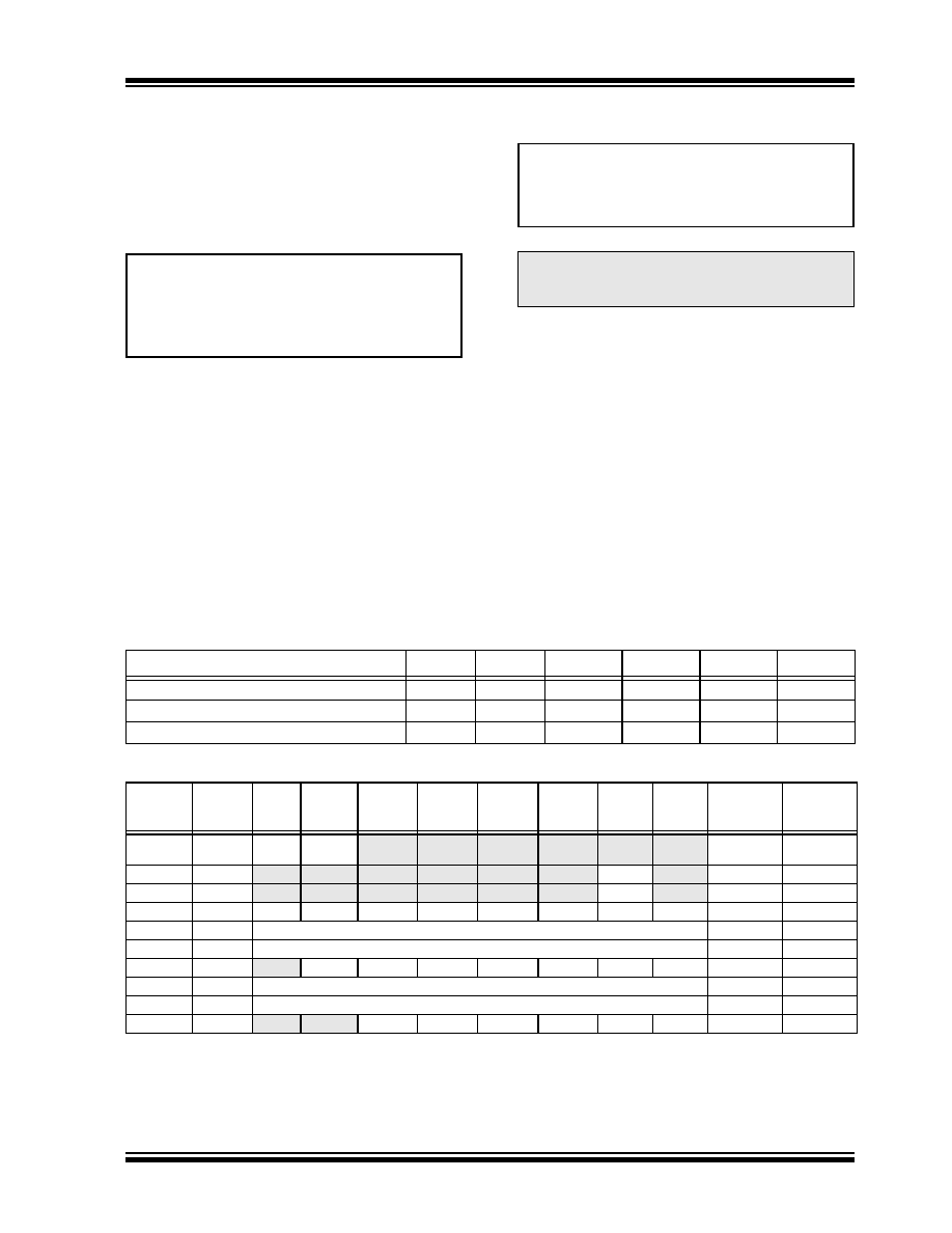
TABLE 9-3:
EXAMPLE PWM FREQUENCIES AND RESOLUTIONS AT 20 MHz
TABLE 9-4:
REGISTERS ASSOCIATED WITH PWM AND TIMER2
(CCPR1L:CCP1CON<5:4>) Tosc TMR2 prescale
value
PWM duty cycle =
Note:
If the PWM duty cycle value is longer than
the PWM period the CCP1 pin will not be
cleared.
Resolution
log
Fosc
FPWM
TMR2 Prescaler
×
-------------------------------------------------------------
log(2)
--------------------------------------------------------------------------- bits
=
PWM
PWM Frequency
1.22 kHz
4.88 kHz
19.53 kHz
78.12 kHz
156.3 kHz
208.3 kHz
Timer Prescaler (1, 4, 16)
16
4
1
PR2 Value
0xFF
0x3F
0x1F
0x17
Maximum Resolution (bits)
10
8
7
6.5
Address
Name
Bit 7
Bit 6
Bit 5
Bit 4
Bit 3
Bit 2
Bit 1
Bit 0
Value on
POR
Value on
all other
Resets
0Bh, 8Bh,
10Bh, 18Bh
INTCON
GIE
PEIE
T0IE
INTE
RBIE
T0IF
INTF
RBIF
0000 000x
0000 000u
0Ch
PIR1
EEIF
CMIF
RCIF
TXIF
—
CCP1IF
TMR2IF
TMR1IF
0000 -000
8Ch
PIE1
EEIE
CMIE
RCIE
TXIE
—
CCP1IE
TMR2IE
TMR1IE
0000 -000
86h, 186h
TRISB
TRISB7
TRISB6
TRISB5
TRISB4
TRISB3
TRISB2
TRISB1
TRISB0
1111 1111
11h
TMR2
Timer2 Module’s Register
0000 0000
92h
PR2
Timer2 Module’s Period Register
1111 1111
12h
T2CON
—
TOUTPS3 TOUTPS2 TOUTPS1 TOUTPS0 TMR2ON T2CKPS1 T2CKPS0 -000 0000
uuuu uuuu
15h
CCPR1L
Capture/Compare/PWM Register 1 (LSB)
xxxx xxxx
uuuu uuuu
16h
CCPR1H
Capture/Compare/PWM Register 1 (MSB)
xxxx xxxx
uuuu uuuu
17h
CCP1CON
—
CCP1X
CCP1Y
CCP1M3
CCP1M2
CCP1M1 CCP1M0
--00 0000
Legend:
x
= unknown, u = unchanged, - = unimplemented read as ‘0’. Shaded cells are not used by PWM and Timer2.
相关PDF资料 |
PDF描述 |
|---|---|
| PIC24F16KA102-E/ML | MCU 16KB FLASH 1.5KB RAM 28QFN |
| PIC24FJ48GA002T-I/SS | IC PIC MCU FLASH 48K 28SSOP |
| VI-J53-IX-S | CONVERTER MOD DC/DC 24V 75W |
| VE-241-IY-B1 | CONVERTER MOD DC/DC 12V 50W |
| VI-BTK-IY-B1 | CONVERTER MOD DC/DC 40V 50W |
相关代理商/技术参数 |
参数描述 |
|---|---|
| PIC16F676-E/ML | 功能描述:8位微控制器 -MCU 1.75KB 64 RAM 12I/O Ext Temp QFN RoHS:否 制造商:Silicon Labs 核心:8051 处理器系列:C8051F39x 数据总线宽度:8 bit 最大时钟频率:50 MHz 程序存储器大小:16 KB 数据 RAM 大小:1 KB 片上 ADC:Yes 工作电源电压:1.8 V to 3.6 V 工作温度范围:- 40 C to + 105 C 封装 / 箱体:QFN-20 安装风格:SMD/SMT |
| PIC16F676-E/P | 功能描述:8位微控制器 -MCU 1.75KB 64 RAM 12 I/O Ext Temp PDIP14 RoHS:否 制造商:Silicon Labs 核心:8051 处理器系列:C8051F39x 数据总线宽度:8 bit 最大时钟频率:50 MHz 程序存储器大小:16 KB 数据 RAM 大小:1 KB 片上 ADC:Yes 工作电源电压:1.8 V to 3.6 V 工作温度范围:- 40 C to + 105 C 封装 / 箱体:QFN-20 安装风格:SMD/SMT |
| PIC16F676-E/SL | 功能描述:8位微控制器 -MCU 1.75KB 64 RAM 12 I/O Ext Temp SOIC14 RoHS:否 制造商:Silicon Labs 核心:8051 处理器系列:C8051F39x 数据总线宽度:8 bit 最大时钟频率:50 MHz 程序存储器大小:16 KB 数据 RAM 大小:1 KB 片上 ADC:Yes 工作电源电压:1.8 V to 3.6 V 工作温度范围:- 40 C to + 105 C 封装 / 箱体:QFN-20 安装风格:SMD/SMT |
| PIC16F676-E/ST | 功能描述:8位微控制器 -MCU 1.75KB 64 RAM 12 I/O Ext Temp TSSOP14 RoHS:否 制造商:Silicon Labs 核心:8051 处理器系列:C8051F39x 数据总线宽度:8 bit 最大时钟频率:50 MHz 程序存储器大小:16 KB 数据 RAM 大小:1 KB 片上 ADC:Yes 工作电源电压:1.8 V to 3.6 V 工作温度范围:- 40 C to + 105 C 封装 / 箱体:QFN-20 安装风格:SMD/SMT |
| PIC16F676-I/ML | 功能描述:8位微控制器 -MCU 1.75 KB 64 RAM 12I/O RoHS:否 制造商:Silicon Labs 核心:8051 处理器系列:C8051F39x 数据总线宽度:8 bit 最大时钟频率:50 MHz 程序存储器大小:16 KB 数据 RAM 大小:1 KB 片上 ADC:Yes 工作电源电压:1.8 V to 3.6 V 工作温度范围:- 40 C to + 105 C 封装 / 箱体:QFN-20 安装风格:SMD/SMT |
发布紧急采购,3分钟左右您将得到回复。