- 您现在的位置:买卖IC网 > PDF目录3880 > PIC16F785-I/ML (Microchip Technology)IC PIC MCU FLASH 2KX14 20QFN PDF资料下载
参数资料
| 型号: | PIC16F785-I/ML |
| 厂商: | Microchip Technology |
| 文件页数: | 13/206页 |
| 文件大小: | 0K |
| 描述: | IC PIC MCU FLASH 2KX14 20QFN |
| 产品培训模块: | Asynchronous Stimulus 8-bit PIC® Microcontroller Portfolio |
| 标准包装: | 91 |
| 系列: | PIC® 16F |
| 核心处理器: | PIC |
| 芯体尺寸: | 8-位 |
| 速度: | 20MHz |
| 外围设备: | 欠压检测/复位,POR,PWM,WDT |
| 输入/输出数: | 17 |
| 程序存储器容量: | 3.5KB(2K x 14) |
| 程序存储器类型: | 闪存 |
| EEPROM 大小: | 256 x 8 |
| RAM 容量: | 128 x 8 |
| 电压 - 电源 (Vcc/Vdd): | 2 V ~ 5.5 V |
| 数据转换器: | A/D 14x10b |
| 振荡器型: | 内部 |
| 工作温度: | -40°C ~ 85°C |
| 封装/外壳: | 20-VFQFN 裸露焊盘 |
| 包装: | 管件 |
| 产品目录页面: | 639 (CN2011-ZH PDF) |
| 配用: | AC164322-ND - MODULE SOCKET MPLAB PM3 28/44QFN |
第1页第2页第3页第4页第5页第6页第7页第8页第9页第10页第11页第12页当前第13页第14页第15页第16页第17页第18页第19页第20页第21页第22页第23页第24页第25页第26页第27页第28页第29页第30页第31页第32页第33页第34页第35页第36页第37页第38页第39页第40页第41页第42页第43页第44页第45页第46页第47页第48页第49页第50页第51页第52页第53页第54页第55页第56页第57页第58页第59页第60页第61页第62页第63页第64页第65页第66页第67页第68页第69页第70页第71页第72页第73页第74页第75页第76页第77页第78页第79页第80页第81页第82页第83页第84页第85页第86页第87页第88页第89页第90页第91页第92页第93页第94页第95页第96页第97页第98页第99页第100页第101页第102页第103页第104页第105页第106页第107页第108页第109页第110页第111页第112页第113页第114页第115页第116页第117页第118页第119页第120页第121页第122页第123页第124页第125页第126页第127页第128页第129页第130页第131页第132页第133页第134页第135页第136页第137页第138页第139页第140页第141页第142页第143页第144页第145页第146页第147页第148页第149页第150页第151页第152页第153页第154页第155页第156页第157页第158页第159页第160页第161页第162页第163页第164页第165页第166页第167页第168页第169页第170页第171页第172页第173页第174页第175页第176页第177页第178页第179页第180页第181页第182页第183页第184页第185页第186页第187页第188页第189页第190页第191页第192页第193页第194页第195页第196页第197页第198页第199页第200页第201页第202页第203页第204页第205页第206页
2008 Microchip Technology Inc.
DS41249E-page 9
PIC16F785/HV785
2.0
MEMORY ORGANIZATION
2.1
Program Memory Organization
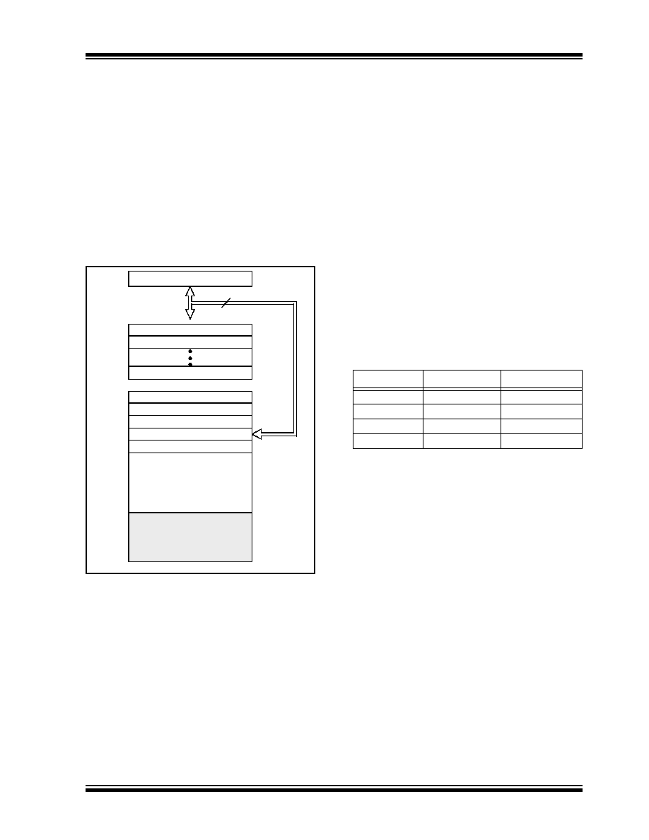
The PIC16F785/HV785 has a 13-bit program counter
capable of addressing an 8k x 14 program memory
space. Only the first 2k x 14 (0000h-07FFh) for the
PIC16F785/HV785 is physically implemented. Access-
ing a location above these boundaries will cause a
wrap around within the first 2k x 14 space. The Reset
vector is at 0000h and the interrupt vector is at 0004h
(see Figure 2-1).
FIGURE 2-1:
PROGRAM MEMORY MAP
AND STACK FOR THE
PIC16F785/HV785
2.2
Data Memory Organization
The data memory (see Figure 2-2) is partitioned into
four banks, which contain the General Purpose
Registers (GPR) and the Special Function Registers
(SFR). The Special Function Registers are located in
the first 32 locations of each bank. Register locations
20h-7Fh in Bank 0 and A0h-BFh in Bank 1 are General
Purpose Registers, implemented as static RAM. The
last sixteen register locations in Bank 1 (F0h-FFh),
Bank 2 (170h-17Fh), and Bank 3 (1F0h-1FFh) point to
addresses 70h-7Fh in Bank 0. All other RAM is
unimplemented and returns ‘0’ when read.
Seven address bits are required to access any location
in a data memory bank. Two additional bits are required
to access the four banks. When data memory is
accessed directly, the seven Least Significant address
bits are contained within the opcode and the two Most
Significant bits are contained in the STATUS register.
RP0 and RP1 bits of the STATUS register are the two
Most Significant data memory address bits and are
also known as the bank select bits. Table 2-1 lists how
to access the four banks of registers.
TABLE 2-1:
BANK SELECTION
2.2.1
GENERAL PURPOSE REGISTER
FILE
The register file banks are organized as 128 x 8 in the
PIC16F785/HV785. Each register is accessed, either
directly, by seven address bits within the opcode, or
indirectly, through the File Select Register (FSR).
When the FSR is used to access data memory, the
eight Least Significant data memory address bits are
contained in the FSR and the ninth Most Significant
address bit is contained in the IRP bit in the STATUS
Register. (see Section 2.4 “Indirect Addressing,
2.2.2
SPECIAL FUNCTION REGISTERS
The Special Function Registers are registers used by
the CPU and peripheral functions for controlling the
desired operation of the device (see Table 2-2). These
registers are static RAM.
The special registers can be classified into two sets:
core and peripheral. The Special Function Registers
associated with the “core” are described in this section.
Those related to the operation of the peripheral
features are described in the section of that peripheral
feature.
PC<12:0>
13
0000h
0004
0005
07FFh
0800h
1FFFh
Stack Level 1
Stack Level 8
Reset Vector
Interrupt Vector
On-chip Program
Memory
CALL, RETURN
RETFIE, RETLW
Stack Level 2
RP1
RP0
Bank 0
00
Bank 1
01
Bank 2
10
Bank 3
11
相关PDF资料 |
PDF描述 |
|---|---|
| XF2L-0425-1 | CONN FPC 4POS 0.5MM SMT |
| PIC16F1933-I/MV | IC MCU 8BIT FLASH 28-UQFN |
| PIC16F785-I/SO | IC PIC MCU FLASH 2KX14 20SOIC |
| PIC16C56A-04/SO | IC MCU OTP 1KX12 18SOIC |
| PIC18F23K20-I/MV | IC MCU 8BIT 8KB FLASH 28UQFN |
相关代理商/技术参数 |
参数描述 |
|---|---|
| PIC16F785T-E/SS | 功能描述:8位微控制器 -MCU 3.5KB FL 128R 18 I/O RoHS:否 制造商:Silicon Labs 核心:8051 处理器系列:C8051F39x 数据总线宽度:8 bit 最大时钟频率:50 MHz 程序存储器大小:16 KB 数据 RAM 大小:1 KB 片上 ADC:Yes 工作电源电压:1.8 V to 3.6 V 工作温度范围:- 40 C to + 105 C 封装 / 箱体:QFN-20 安装风格:SMD/SMT |
| PIC16F785T-I/ML | 功能描述:8位微控制器 -MCU 3.5 KB 128 RAM 18I/O RoHS:否 制造商:Silicon Labs 核心:8051 处理器系列:C8051F39x 数据总线宽度:8 bit 最大时钟频率:50 MHz 程序存储器大小:16 KB 数据 RAM 大小:1 KB 片上 ADC:Yes 工作电源电压:1.8 V to 3.6 V 工作温度范围:- 40 C to + 105 C 封装 / 箱体:QFN-20 安装风格:SMD/SMT |
| PIC16F785T-I/ML036 | 制造商:Microchip Technology Inc 功能描述: |
| PIC16F785T-I/ML045 | 制造商:Microchip Technology Inc 功能描述: |
| PIC16F785T-I/SO | 功能描述:8位微控制器 -MCU 3.5KB FL 128R 18 I/O RoHS:否 制造商:Silicon Labs 核心:8051 处理器系列:C8051F39x 数据总线宽度:8 bit 最大时钟频率:50 MHz 程序存储器大小:16 KB 数据 RAM 大小:1 KB 片上 ADC:Yes 工作电源电压:1.8 V to 3.6 V 工作温度范围:- 40 C to + 105 C 封装 / 箱体:QFN-20 安装风格:SMD/SMT |
发布紧急采购,3分钟左右您将得到回复。