参数资料
| 型号: | PIC16F84-04/P |
| 厂商: | Microchip Technology |
| 文件页数: | 7/80页 |
| 文件大小: | 0K |
| 描述: | IC MCU FLASH 1KX14 EE 18DIP |
| 产品培训模块: | Asynchronous Stimulus 8-bit PIC® Microcontroller Portfolio |
| 标准包装: | 25 |
| 系列: | PIC® 16F |
| 核心处理器: | PIC |
| 芯体尺寸: | 8-位 |
| 速度: | 4MHz |
| 外围设备: | POR,WDT |
| 输入/输出数: | 13 |
| 程序存储器容量: | 1.75KB(1K x 14) |
| 程序存储器类型: | 闪存 |
| EEPROM 大小: | 64 x 8 |
| RAM 容量: | 68 x 8 |
| 电压 - 电源 (Vcc/Vdd): | 4 V ~ 6 V |
| 振荡器型: | 外部 |
| 工作温度: | 0°C ~ 70°C |
| 封装/外壳: | 18-DIP(0.300",7.62mm) |
| 包装: | 管件 |
| 配用: | DVA16XP180-ND - ADAPTER DEVICE FOR MPLAB-ICE AC164010-ND - MODULE SKT PROMATEII DIP/SOIC |
第1页第2页第3页第4页第5页第6页当前第7页第8页第9页第10页第11页第12页第13页第14页第15页第16页第17页第18页第19页第20页第21页第22页第23页第24页第25页第26页第27页第28页第29页第30页第31页第32页第33页第34页第35页第36页第37页第38页第39页第40页第41页第42页第43页第44页第45页第46页第47页第48页第49页第50页第51页第52页第53页第54页第55页第56页第57页第58页第59页第60页第61页第62页第63页第64页第65页第66页第67页第68页第69页第70页第71页第72页第73页第74页第75页第76页第77页第78页第79页第80页
PIC16F8X
1998 Microchip Technology Inc.
DS30430C-page 15
4.2.2.1
STATUS REGISTER
The STATUS register contains the arithmetic status of
the ALU, the RESET status and the bank select bit for
data memory.
As with any register, the STATUS register can be the
destination for any instruction. If the STATUS register is
the destination for an instruction that affects the Z, DC
or C bits, then the write to these three bits is disabled.
These bits are set or cleared according to device logic.
Furthermore, the TO and PD bits are not writable.
Therefore, the result of an instruction with the STATUS
register as destination may be different than intended.
For example, CLRF STATUS will clear the upper-three
bits and set the Z bit. This leaves the STATUS register
as 000u u1uu (where u = unchanged).
Only the BCF, BSF, SWAPF and MOVWF instructions
should be used to alter the STATUS register (Table 9-2)
because these instructions do not affect any status bit.
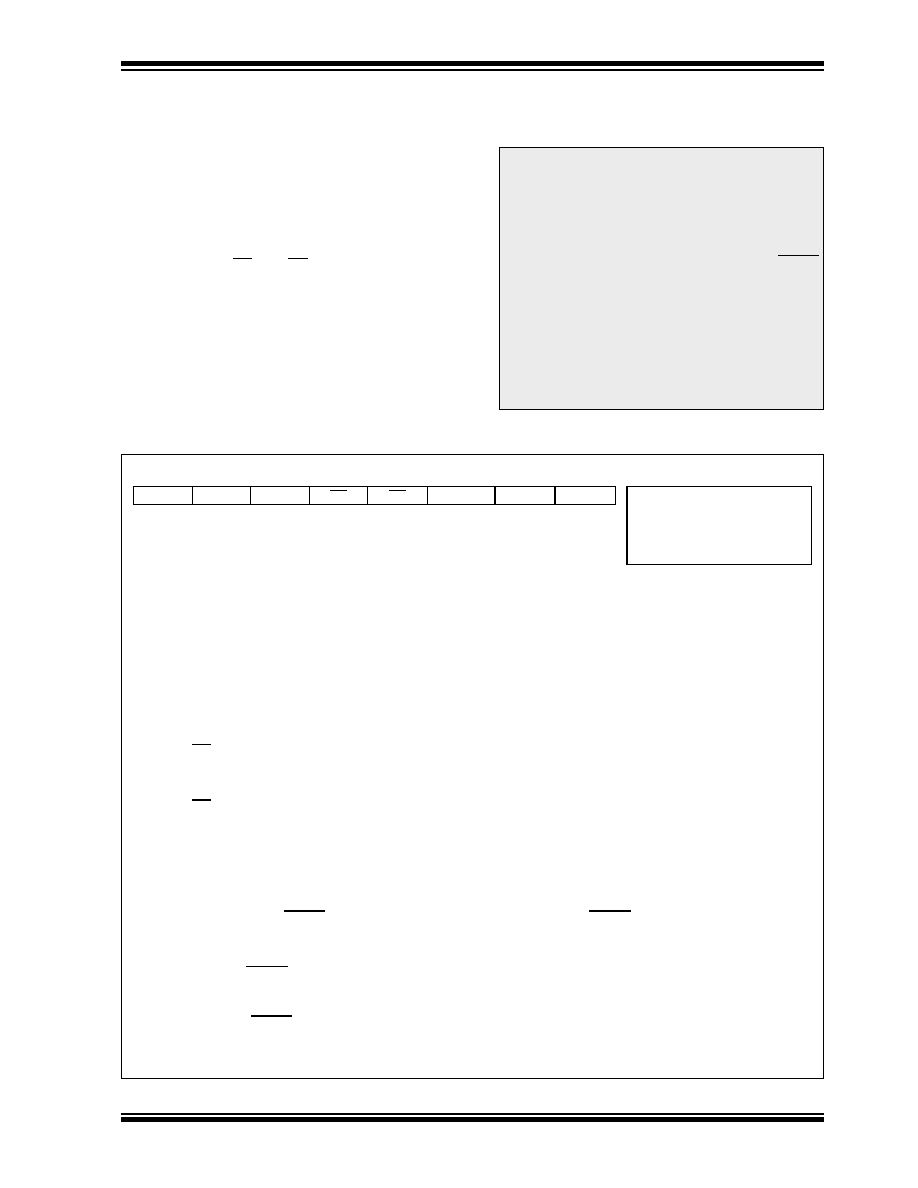
FIGURE 4-1:
STATUS REGISTER (ADDRESS 03h, 83h)
Note 1: The IRP and RP1 bits (STATUS<7:6>) are
not used by the PIC16F8X and should be
programmed as cleared. Use of these bits
as general purpose R/W bits is NOT
recommended, since this may affect
upward compatibility with future products.
Note 2: The C and DC bits operate as a borrow
and digit borrow out bit, respectively, in
subtraction. See the SUBLW and SUBWF
instructions for examples.
Note 3: When
the
STATUS
register
is
the
destination for an instruction that affects
the Z, DC or C bits, then the write to these
three bits is disabled. The specified bit(s)
will be updated according to device logic
R/W-0
R-1
R/W-x
IRP
RP1
RP0
TO
PD
Z
DC
C
R = Readable bit
W = Writable bit
U = Unimplemented bit,
read as ‘0’
- n = Value at POR reset
bit7
bit0
bit 7:
IRP: Register Bank Select bit (used for indirect addressing)
0 = Bank 0, 1 (00h - FFh)
1 = Bank 2, 3 (100h - 1FFh)
The IRP bit is not used by the PIC16F8X. IRP should be maintained clear.
bit 6-5: RP1:RP0: Register Bank Select bits (used for direct addressing)
00 = Bank 0 (00h - 7Fh)
01 = Bank 1 (80h - FFh)
10 = Bank 2 (100h - 17Fh)
11 = Bank 3 (180h - 1FFh)
Each bank is 128 bytes. Only bit RP0 is used by the PIC16F8X. RP1 should be maintained clear.
bit 4:
TO: Time-out bit
1 = After power-up, CLRWDT instruction, or SLEEP instruction
0 = A WDT time-out occurred
bit 3:
PD: Power-down bit
1 = After power-up or by the CLRWDT instruction
0 = By execution of the SLEEP instruction
bit 2:
Z: Zero bit
1 = The result of an arithmetic or logic operation is zero
0 = The result of an arithmetic or logic operation is not zero
bit 1:
DC: Digit carry/borrow bit (for ADDWF and ADDLW instructions) (For borrow the polarity is reversed)
1 = A carry-out from the 4th low order bit of the result occurred
0 = No carry-out from the 4th low order bit of the result
bit 0:
C: Carry/borrow bit (for ADDWF and ADDLW instructions)
1 = A carry-out from the most significant bit of the result occurred
0 = No carry-out from the most significant bit of the result occurred
Note:For borrow the polarity is reversed. A subtraction is executed by adding the two’s complement of
the second operand. For rotate (RRF, RLF) instructions, this bit is loaded with either the high or low
order bit of the source register.
相关PDF资料 |
PDF描述 |
|---|---|
| PIC24HJ128GP202-I/SO | IC PIC MCU FLASH 128K 28SOIC |
| PIC24FJ128GA310-I/PT | MCU 16BIT 128KB FLASH 100TQFP |
| DSPIC33FJ16GS504-I/PT | IC DSPIC MCU/DSP 16K 44-TQFP |
| DSPIC33FJ64GP802-I/SO | IC DSPIC MCU/DSP 64K 28-SOIC |
| AT89LP4052-16XU | IC 8051 MCU FLASH 4K 20TSSOP |
相关代理商/技术参数 |
参数描述 |
|---|---|
| PIC16F84-10/P | 功能描述:8位微控制器 -MCU 1.75KB 68 RAM 13 I/O 10MHz PDIP18 RoHS:否 制造商:Silicon Labs 核心:8051 处理器系列:C8051F39x 数据总线宽度:8 bit 最大时钟频率:50 MHz 程序存储器大小:16 KB 数据 RAM 大小:1 KB 片上 ADC:Yes 工作电源电压:1.8 V to 3.6 V 工作温度范围:- 40 C to + 105 C 封装 / 箱体:QFN-20 安装风格:SMD/SMT |
| PIC16F84-10/P | 制造商:Microchip Technology Inc 功能描述:IC 8-BIT FLASH MCU |
| PIC16F84-10/SO | 功能描述:8位微控制器 -MCU 1.75KB 68 RAM 13 I/O 10MHz SOIC18 RoHS:否 制造商:Silicon Labs 核心:8051 处理器系列:C8051F39x 数据总线宽度:8 bit 最大时钟频率:50 MHz 程序存储器大小:16 KB 数据 RAM 大小:1 KB 片上 ADC:Yes 工作电源电压:1.8 V to 3.6 V 工作温度范围:- 40 C to + 105 C 封装 / 箱体:QFN-20 安装风格:SMD/SMT |
| PIC16F84-10/SO | 制造商:Microchip Technology Inc 功能描述:IC SM 8-BIT FLASH MCU |
| PIC16F84-10I/P | 功能描述:8位微控制器 -MCU 1.75KB 68 RAM 13 I/O 10MHz IndTemp PDIP18 RoHS:否 制造商:Silicon Labs 核心:8051 处理器系列:C8051F39x 数据总线宽度:8 bit 最大时钟频率:50 MHz 程序存储器大小:16 KB 数据 RAM 大小:1 KB 片上 ADC:Yes 工作电源电压:1.8 V to 3.6 V 工作温度范围:- 40 C to + 105 C 封装 / 箱体:QFN-20 安装风格:SMD/SMT |
发布紧急采购,3分钟左右您将得到回复。