- 您现在的位置:买卖IC网 > PDF目录3882 > PIC16F87T-I/ML (Microchip Technology)IC MCU FLASH 4KX14 EEPROM 28QFN PDF资料下载
参数资料
| 型号: | PIC16F87T-I/ML |
| 厂商: | Microchip Technology |
| 文件页数: | 38/200页 |
| 文件大小: | 0K |
| 描述: | IC MCU FLASH 4KX14 EEPROM 28QFN |
| 标准包装: | 1,600 |
| 系列: | PIC® 16F |
| 核心处理器: | PIC |
| 芯体尺寸: | 8-位 |
| 速度: | 20MHz |
| 连通性: | I²C,SPI,UART/USART |
| 外围设备: | 欠压检测/复位,POR,PWM,WDT |
| 输入/输出数: | 16 |
| 程序存储器容量: | 7KB(4K x 14) |
| 程序存储器类型: | 闪存 |
| EEPROM 大小: | 256 x 8 |
| RAM 容量: | 368 x 8 |
| 电压 - 电源 (Vcc/Vdd): | 4 V ~ 5.5 V |
| 振荡器型: | 内部 |
| 工作温度: | -40°C ~ 85°C |
| 封装/外壳: | 28-VQFN 裸露焊盘 |
| 包装: | 带卷 (TR) |
| 配用: | XLT28QFN3-ND - SOCKET TRAN ICE 18DIP/28QFN AC164033-ND - ADAPTER 28QFN TO 18DIP |
第1页第2页第3页第4页第5页第6页第7页第8页第9页第10页第11页第12页第13页第14页第15页第16页第17页第18页第19页第20页第21页第22页第23页第24页第25页第26页第27页第28页第29页第30页第31页第32页第33页第34页第35页第36页第37页当前第38页第39页第40页第41页第42页第43页第44页第45页第46页第47页第48页第49页第50页第51页第52页第53页第54页第55页第56页第57页第58页第59页第60页第61页第62页第63页第64页第65页第66页第67页第68页第69页第70页第71页第72页第73页第74页第75页第76页第77页第78页第79页第80页第81页第82页第83页第84页第85页第86页第87页第88页第89页第90页第91页第92页第93页第94页第95页第96页第97页第98页第99页第100页第101页第102页第103页第104页第105页第106页第107页第108页第109页第110页第111页第112页第113页第114页第115页第116页第117页第118页第119页第120页第121页第122页第123页第124页第125页第126页第127页第128页第129页第130页第131页第132页第133页第134页第135页第136页第137页第138页第139页第140页第141页第142页第143页第144页第145页第146页第147页第148页第149页第150页第151页第152页第153页第154页第155页第156页第157页第158页第159页第160页第161页第162页第163页第164页第165页第166页第167页第168页第169页第170页第171页第172页第173页第174页第175页第176页第177页第178页第179页第180页第181页第182页第183页第184页第185页第186页第187页第188页第189页第190页第191页第192页第193页第194页第195页第196页第197页第198页第199页第200页
132
8008H–AVR–04/11
ATtiny48/88
The MSB of the address byte is transmitted first. Slave addresses can freely be allocated by the
designer, but the address 0000 000 is reserved for a general call.
When a general call is issued, all slaves should respond by pulling the SDA line low in the ACK
cycle. A general call is used when a Master wishes to transmit the same message to several
slaves in the system. When the general call address followed by a Write bit is transmitted on the
bus, all slaves set up to acknowledge the general call will pull the SDA line low in the ack cycle.
The following data packets will then be received by all the slaves that acknowledged the general
call. Note that transmitting the general call address followed by a Read bit is meaningless, as
this would cause contention if several slaves started transmitting different data.
All addresses of the format 1111 xxx should be reserved for future purposes.
15.4.4
Data Packet Format
All data packets transmitted on the TWI bus are nine bits long, consisting of one data byte and
an acknowledge bit. During a data transfer, the Master generates the clock and the START and
STOP conditions, while the Receiver is responsible for acknowledging the reception. An
Acknowledge (ACK) is signalled by the Receiver pulling the SDA line low during the ninth SCL
cycle. If the Receiver leaves the SDA line high, a NACK is signalled. When the Receiver has
received the last byte, or for some reason cannot receive any more bytes, it should inform the
Transmitter by sending a NACK after the final byte. The MSB of the data byte is transmitted first.
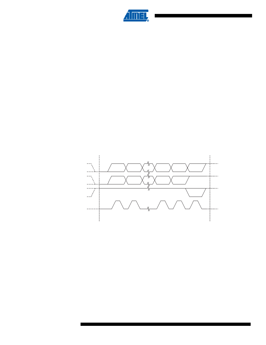
Figure 15-5. Data Packet Format
15.4.5
Combining Address and Data Packets into a Transmission
A transmission basically consists of a START condition, a SLA+R/W, one or more data packets
and a STOP condition. An empty message, consisting of a START followed by a STOP condi-
tion, is illegal. Note that the Wired-ANDing of the SCL line can be used to implement
handshaking between the Master and the Slave. The Slave can extend the SCL low period by
pulling the SCL line low. This is useful if the clock speed set up by the Master is too fast for the
Slave, or the Slave needs extra time for processing between the data transmissions. The Slave
extending the SCL low period will not affect the SCL high period, which is determined by the
Master. As a consequence, the Slave can reduce the TWI data transfer speed by prolonging the
SCL duty cycle.
Figure 15-6 shows a typical data transmission. Note that several data bytes can be transmitted
between the SLA+R/W and the STOP condition, depending on the software protocol imple-
mented by the application software.
12
78
9
Data MSB
Data LSB
ACK
Aggregate
SDA
SDA from
Transmitter
SDA from
Receiver
SCL from
Master
SLA+R/W
Data Byte
STOP, REPEATED
START or Next
Data Byte
相关PDF资料 |
PDF描述 |
|---|---|
| PIC16F87T-E/ML | IC MCU FLASH 4KX14 EEPROM 28QFN |
| PIC16F87-E/ML | IC MCU FLASH 4KX14 EEPROM 28QFN |
| PIC18LF4320-I/ML | IC MCU FLASH 4KX16 EEPROM 44QFN |
| PIC16F77T-I/PTG | IC MCU FLASH 8KX14 W/AD 44TQFP |
| PIC16LF1933-I/SO | IC PIC MCU FLASH 4K 28-SOIC |
相关代理商/技术参数 |
参数描述 |
|---|---|
| PIC16F882-E/ML | 功能描述:8位微控制器 -MCU 3.5KB Enh FLSH 128 RAM RoHS:否 制造商:Silicon Labs 核心:8051 处理器系列:C8051F39x 数据总线宽度:8 bit 最大时钟频率:50 MHz 程序存储器大小:16 KB 数据 RAM 大小:1 KB 片上 ADC:Yes 工作电源电压:1.8 V to 3.6 V 工作温度范围:- 40 C to + 105 C 封装 / 箱体:QFN-20 安装风格:SMD/SMT |
| PIC16F882-E/SO | 功能描述:8位微控制器 -MCU 3.5KB Enh FLSH 128 RAM RoHS:否 制造商:Silicon Labs 核心:8051 处理器系列:C8051F39x 数据总线宽度:8 bit 最大时钟频率:50 MHz 程序存储器大小:16 KB 数据 RAM 大小:1 KB 片上 ADC:Yes 工作电源电压:1.8 V to 3.6 V 工作温度范围:- 40 C to + 105 C 封装 / 箱体:QFN-20 安装风格:SMD/SMT |
| PIC16F882-E/SP | 功能描述:8位微控制器 -MCU 3.5KB Enh FLSH 128 RAM RoHS:否 制造商:Silicon Labs 核心:8051 处理器系列:C8051F39x 数据总线宽度:8 bit 最大时钟频率:50 MHz 程序存储器大小:16 KB 数据 RAM 大小:1 KB 片上 ADC:Yes 工作电源电压:1.8 V to 3.6 V 工作温度范围:- 40 C to + 105 C 封装 / 箱体:QFN-20 安装风格:SMD/SMT |
| PIC16F882-E/SS | 功能描述:8位微控制器 -MCU 3.5KB Enh FLSH 128 RAM RoHS:否 制造商:Silicon Labs 核心:8051 处理器系列:C8051F39x 数据总线宽度:8 bit 最大时钟频率:50 MHz 程序存储器大小:16 KB 数据 RAM 大小:1 KB 片上 ADC:Yes 工作电源电压:1.8 V to 3.6 V 工作温度范围:- 40 C to + 105 C 封装 / 箱体:QFN-20 安装风格:SMD/SMT |
| PIC16F882-I/ML | 功能描述:8位微控制器 -MCU 3.5KB Enh FLSH 128 RAM RoHS:否 制造商:Silicon Labs 核心:8051 处理器系列:C8051F39x 数据总线宽度:8 bit 最大时钟频率:50 MHz 程序存储器大小:16 KB 数据 RAM 大小:1 KB 片上 ADC:Yes 工作电源电压:1.8 V to 3.6 V 工作温度范围:- 40 C to + 105 C 封装 / 箱体:QFN-20 安装风格:SMD/SMT |
发布紧急采购,3分钟左右您将得到回复。