- 您现在的位置:买卖IC网 > PDF目录11500 > PIC16F913-E/ML (Microchip Technology)IC PIC MCU FLASH 4KX14 28QFN PDF资料下载
参数资料
| 型号: | PIC16F913-E/ML |
| 厂商: | Microchip Technology |
| 文件页数: | 27/229页 |
| 文件大小: | 0K |
| 描述: | IC PIC MCU FLASH 4KX14 28QFN |
| 产品培训模块: | Asynchronous Stimulus |
| 标准包装: | 61 |
| 系列: | PIC® 16F |
| 核心处理器: | PIC |
| 芯体尺寸: | 8-位 |
| 速度: | 20MHz |
| 连通性: | I²C,SPI,UART/USART |
| 外围设备: | 欠压检测/复位,LCD,POR,PWM,WDT |
| 输入/输出数: | 24 |
| 程序存储器容量: | 7KB(4K x 14) |
| 程序存储器类型: | 闪存 |
| EEPROM 大小: | 256 x 8 |
| RAM 容量: | 256 x 8 |
| 电压 - 电源 (Vcc/Vdd): | 2 V ~ 5.5 V |
| 数据转换器: | A/D 5x10b |
| 振荡器型: | 内部 |
| 工作温度: | -40°C ~ 125°C |
| 封装/外壳: | 28-VQFN 裸露焊盘 |
| 包装: | 管件 |
第1页第2页第3页第4页第5页第6页第7页第8页第9页第10页第11页第12页第13页第14页第15页第16页第17页第18页第19页第20页第21页第22页第23页第24页第25页第26页当前第27页第28页第29页第30页第31页第32页第33页第34页第35页第36页第37页第38页第39页第40页第41页第42页第43页第44页第45页第46页第47页第48页第49页第50页第51页第52页第53页第54页第55页第56页第57页第58页第59页第60页第61页第62页第63页第64页第65页第66页第67页第68页第69页第70页第71页第72页第73页第74页第75页第76页第77页第78页第79页第80页第81页第82页第83页第84页第85页第86页第87页第88页第89页第90页第91页第92页第93页第94页第95页第96页第97页第98页第99页第100页第101页第102页第103页第104页第105页第106页第107页第108页第109页第110页第111页第112页第113页第114页第115页第116页第117页第118页第119页第120页第121页第122页第123页第124页第125页第126页第127页第128页第129页第130页第131页第132页第133页第134页第135页第136页第137页第138页第139页第140页第141页第142页第143页第144页第145页第146页第147页第148页第149页第150页第151页第152页第153页第154页第155页第156页第157页第158页第159页第160页第161页第162页第163页第164页第165页第166页第167页第168页第169页第170页第171页第172页第173页第174页第175页第176页第177页第178页第179页第180页第181页第182页第183页第184页第185页第186页第187页第188页第189页第190页第191页第192页第193页第194页第195页第196页第197页第198页第199页第200页第201页第202页第203页第204页第205页第206页第207页第208页第209页第210页第211页第212页第213页第214页第215页第216页第217页第218页第219页第220页第221页第222页第223页第224页第225页第226页第227页第228页第229页
207
8018P–AVR–08/10
ATmega169P
20.4
USI Register Descriptions
20.4.1
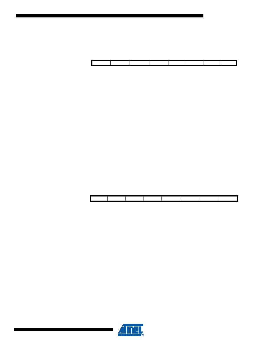
USIDR – USI Data Register
The USI uses no buffering of the Serial Register, that is, when accessing the Data Register
(USIDR) the Serial Register is accessed directly. If a serial clock occurs at the same cycle the
register is written, the register will contain the value written and no shift is performed. A (left) shift
operation is performed depending of the USICS1..0 bits setting. The shift operation can be con-
trolled by an external clock edge, by a Timer/Counter0 Compare Match, or directly by software
using the USICLK strobe bit. Note that even when no wire mode is selected (USIWM1..0 = 0)
both the external data input (DI/SDA) and the external clock input (USCK/SCL) can still be used
by the Shift Register.
The output pin in use, DO or SDA depending on the wire mode, is connected via the output latch
to the most significant bit (bit 7) of the Data Register. The output latch is open (transparent) dur-
ing the first half of a serial clock cycle when an external clock source is selected (USICS1 = 1),
and constantly open when an internal clock source is used (USICS1 = 0). The output will be
changed immediately when a new MSB written as long as the latch is open. The latch ensures
that data input is sampled and data output is changed on opposite clock edges.
Note that the corresponding Data Direction Register to the pin must be set to one for enabling
data output from the Shift Register.
20.4.2
USISR – USI Status Register
The Status Register contains Interrupt Flags, line Status Flags and the counter value.
Bit 7 – USISIF: Start Condition Interrupt Flag
When Two-wire mode is selected, the USISIF Flag is set (to one) when a start condition is
detected. When output disable mode or Three-wire mode is selected and (USICSx = 0b11 &
USICLK = 0) or (USICS = 0b10 & USICLK = 0), any edge on the SCK pin sets the flag.
An interrupt will be generated when the flag is set while the USISIE bit in USICR and the Global
Interrupt Enable Flag are set. The flag will only be cleared by writing a logical one to the USISIF
bit. Clearing this bit will release the start detection hold of USCL in Two-wire mode.
A start condition interrupt will wakeup the processor from all sleep modes.
Bit 6 – USIOIF: Counter Overflow Interrupt Flag
This flag is set (one) when the 4-bit counter overflows (that is, at the transition from 15 to 0). An
interrupt will be generated when the flag is set while the USIOIE bit in USICR and the Global
Interrupt Enable Flag are set. The flag will only be cleared if a one is written to the USIOIF bit.
Clearing this bit will release the counter overflow hold of SCL in Two-wire mode.
Bit
7
6
5
4
3
2
1
0
(0xBA)
MSB
LSB
USIDR
Read/Write
R/W
Initial Value
0
Bit
7
6
5
4
3
210
(0xB9)
USISIF
USIOIF
USIPF
USIDC
USICNT3
USICNT2
USICNT1
USICNT0
USISR
Read/Write
R/W
R
R/W
Initial Value
0
相关PDF资料 |
PDF描述 |
|---|---|
| ADG719BRTZ-REEL7 | IC SWITCH SPDT SOT23-6 |
| PIC24FV16KA301-E/SO | IC MCU 16B 16KB FLASH 20SOIC |
| ADG702BRJZ-REEL7 | IC SWITCH SPST SOT23-5 |
| VI-B3B-CU-F2 | CONVERTER MOD DC/DC 95V 200W |
| PIC24F16KA301-E/SO | IC MCU 16BIT 16KB FLASH 20SOIC |
相关代理商/技术参数 |
参数描述 |
|---|---|
| PIC16F913-I/ML | 功能描述:8位微控制器 -MCU 7KB FL 352R 25 I/O RoHS:否 制造商:Silicon Labs 核心:8051 处理器系列:C8051F39x 数据总线宽度:8 bit 最大时钟频率:50 MHz 程序存储器大小:16 KB 数据 RAM 大小:1 KB 片上 ADC:Yes 工作电源电压:1.8 V to 3.6 V 工作温度范围:- 40 C to + 105 C 封装 / 箱体:QFN-20 安装风格:SMD/SMT |
| PIC16F913-I/SO | 功能描述:8位微控制器 -MCU 7KB FL 352R 25 I/O RoHS:否 制造商:Silicon Labs 核心:8051 处理器系列:C8051F39x 数据总线宽度:8 bit 最大时钟频率:50 MHz 程序存储器大小:16 KB 数据 RAM 大小:1 KB 片上 ADC:Yes 工作电源电压:1.8 V to 3.6 V 工作温度范围:- 40 C to + 105 C 封装 / 箱体:QFN-20 安装风格:SMD/SMT |
| PIC16F913-I/SO | 制造商:Microchip Technology Inc 功能描述:8 Bit Microcontroller Clock Speed:20MHz |
| PIC16F913-I/SP | 功能描述:8位微控制器 -MCU 7KB FL 352R 25 I/O RoHS:否 制造商:Silicon Labs 核心:8051 处理器系列:C8051F39x 数据总线宽度:8 bit 最大时钟频率:50 MHz 程序存储器大小:16 KB 数据 RAM 大小:1 KB 片上 ADC:Yes 工作电源电压:1.8 V to 3.6 V 工作温度范围:- 40 C to + 105 C 封装 / 箱体:QFN-20 安装风格:SMD/SMT |
| PIC16F913-I/SP | 制造商:Microchip Technology Inc 功能描述:8 Bit Microcontroller Clock Speed:20MHz |
发布紧急采购,3分钟左右您将得到回复。