- 您现在的位置:买卖IC网 > PDF目录11575 > PIC16HV540T-04/SO (Microchip Technology)IC MCU OTP 512X12 18SOIC PDF资料下载
参数资料
| 型号: | PIC16HV540T-04/SO |
| 厂商: | Microchip Technology |
| 文件页数: | 2/44页 |
| 文件大小: | 0K |
| 描述: | IC MCU OTP 512X12 18SOIC |
| 产品培训模块: | Asynchronous Stimulus |
| 标准包装: | 1,100 |
| 系列: | PIC® 16C |
| 核心处理器: | PIC |
| 芯体尺寸: | 8-位 |
| 速度: | 4MHz |
| 外围设备: | 欠压检测/复位,POR,WDT |
| 输入/输出数: | 12 |
| 程序存储器容量: | 768B(512 x 12) |
| 程序存储器类型: | OTP |
| RAM 容量: | 25 x 8 |
| 电压 - 电源 (Vcc/Vdd): | 3.5 V ~ 15 V |
| 振荡器型: | 外部 |
| 工作温度: | 0°C ~ 70°C |
| 封装/外壳: | 18-SOIC(0.295",7.50mm 宽) |
| 包装: | 带卷 (TR) |
第1页当前第2页第3页第4页第5页第6页第7页第8页第9页第10页第11页第12页第13页第14页第15页第16页第17页第18页第19页第20页第21页第22页第23页第24页第25页第26页第27页第28页第29页第30页第31页第32页第33页第34页第35页第36页第37页第38页第39页第40页第41页第42页第43页第44页
PIC16HV540
DS40197B-page 10
Preliminary
2000 Microchip Technology Inc.
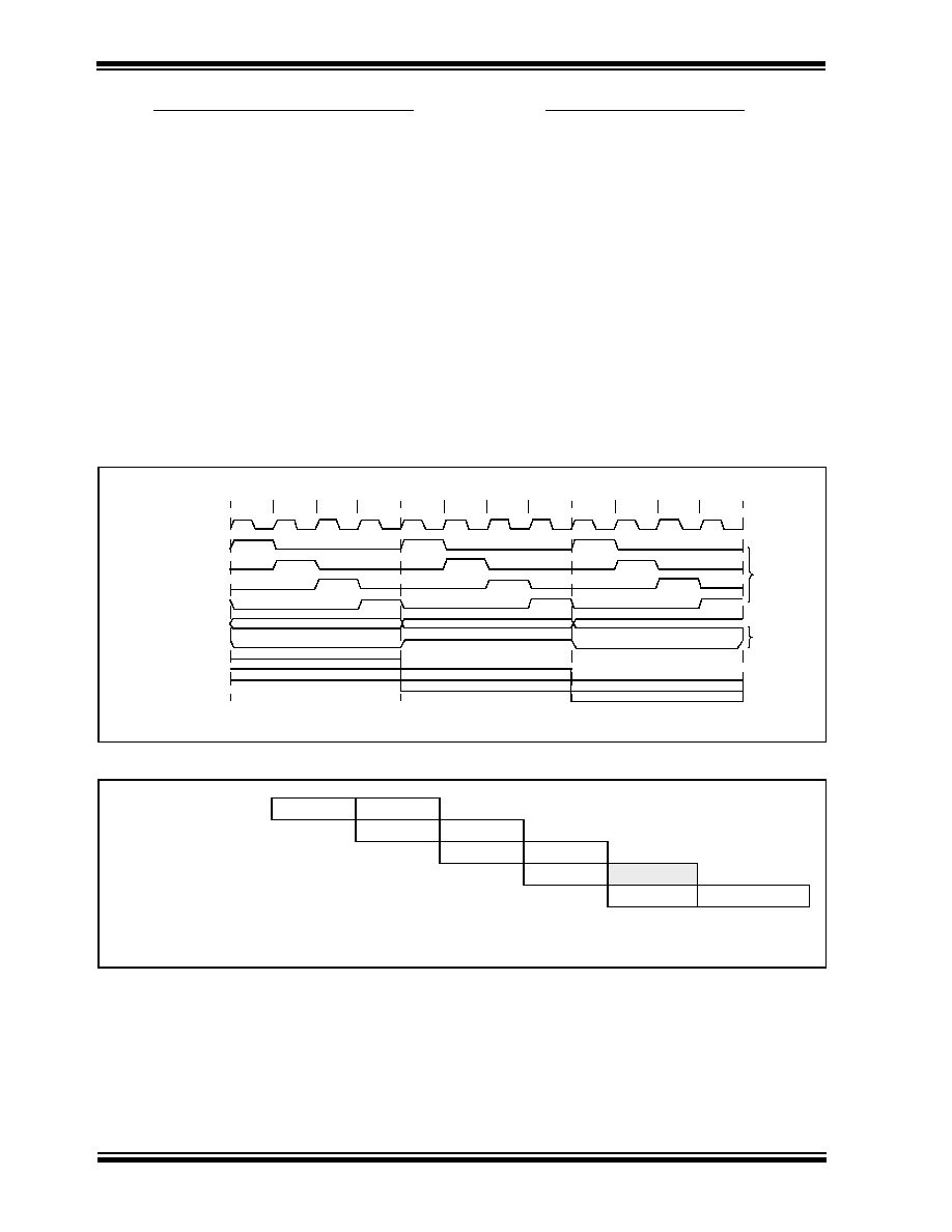
3.1
Clocking Scheme/Instruction Cycle
The clock input (OSC1/CLKIN pin) is internally divided
by four to generate four non-overlapping quadrature
clocks namely Q1, Q2, Q3 and Q4. Internally, the pro-
gram counter is incremented every Q1, and the instruc-
tion is fetched from program memory and latched into
instruction register in Q4. It is decoded and executed
during the following Q1 through Q4. The clocks and
instruction execution flow is shown in Figure 3-2 and
3.2
Instruction Flow/Pipelining
An Instruction Cycle consists of four Q cycles (Q1, Q2,
Q3 and Q4). The instruction fetch and execute are
pipelined such that fetch takes one instruction cycle
while decode and execute takes another instruction
cycle. However, due to the pipelining, each instruction
effectively executes in one cycle. If an instruction
causes the program counter to change (e.g., GOTO)
then two cycles are required to complete the instruction
A fetch cycle begins with the program counter (PC)
incrementing in Q1.
In the execution cycle, the fetched instruction is latched
into the Instruction Register (IR) in cycle Q1. This
instruction is then decoded and executed during the
Q2, Q3, and Q4 cycles. Data memory is read during Q2
(operand read) and written during Q4 (destination
write).
FIGURE 3-2:
CLOCK/INSTRUCTION CYCLE
EXAMPLE 3-1:
INSTRUCTION PIPELINE FLOW
Q1
Q2
Q3
Q4
Q1
Q2
Q3
Q4
Q1
Q2
Q3
Q4
OSC1
Q1
Q2
Q3
Q4
PC
OSC2/CLKOUT
(RC mode)
PC
PC+1
PC+2
Fetch INST (PC)
Execute INST (PC-1)
Fetch INST (PC+1)
Execute INST (PC)
Fetch INST (PC+2)
Execute INST (PC+1)
Internal
phase
clock
Note 1: Frequencies of CLKIN8 to CLKIN/1024 are possible.
CLKIN/8(1)
All instructions are single cycle, except for any program branches. These take two cycles since the fetch instruction is “flushed”
from the pipeline while the new instruction is being fetched and then executed.
1. MOVLW 55H
Fetch 1
Execute 1
2. MOVWF PORTB
Fetch 2
Execute 2
3. CALL
SUB_1
Fetch 3
Execute 3
4. BSF
PORTA, BIT3
Fetch 4
Flush
Fetch SUB_1 Execute SUB_1
相关PDF资料 |
PDF描述 |
|---|---|
| V300A5C400B | CONVERTER MOD DC/DC 5V 400W |
| V300A8C400BG2 | CONVERTER MOD DC/DC 8V 400W |
| KSZ8873MLLI | IC ETHERNET SWITCH 3PORT 64LQFP |
| KSZ8873MLL AM TR | IC ETHERNET SWITCH 3PORT 64LQFP |
| PIC16C54CT-04I/SO | IC MCU OTP 512X12 18SOIC |
相关代理商/技术参数 |
参数描述 |
|---|---|
| PIC16HV540T-20/SO | 功能描述:8位微控制器 -MCU .75KB 25 RAM 12 I/O RoHS:否 制造商:Silicon Labs 核心:8051 处理器系列:C8051F39x 数据总线宽度:8 bit 最大时钟频率:50 MHz 程序存储器大小:16 KB 数据 RAM 大小:1 KB 片上 ADC:Yes 工作电源电压:1.8 V to 3.6 V 工作温度范围:- 40 C to + 105 C 封装 / 箱体:QFN-20 安装风格:SMD/SMT |
| PIC16HV540T-20/SS | 功能描述:8位微控制器 -MCU .75KB 25 RAM 12 I/O RoHS:否 制造商:Silicon Labs 核心:8051 处理器系列:C8051F39x 数据总线宽度:8 bit 最大时钟频率:50 MHz 程序存储器大小:16 KB 数据 RAM 大小:1 KB 片上 ADC:Yes 工作电源电压:1.8 V to 3.6 V 工作温度范围:- 40 C to + 105 C 封装 / 箱体:QFN-20 安装风格:SMD/SMT |
| PIC16HV540T-20I/SO | 功能描述:8位微控制器 -MCU .75KB 25 RAM 12 I/O RoHS:否 制造商:Silicon Labs 核心:8051 处理器系列:C8051F39x 数据总线宽度:8 bit 最大时钟频率:50 MHz 程序存储器大小:16 KB 数据 RAM 大小:1 KB 片上 ADC:Yes 工作电源电压:1.8 V to 3.6 V 工作温度范围:- 40 C to + 105 C 封装 / 箱体:QFN-20 安装风格:SMD/SMT |
| PIC16HV540T-20I/SS | 功能描述:8位微控制器 -MCU .75KB 25 RAM 12 I/O RoHS:否 制造商:Silicon Labs 核心:8051 处理器系列:C8051F39x 数据总线宽度:8 bit 最大时钟频率:50 MHz 程序存储器大小:16 KB 数据 RAM 大小:1 KB 片上 ADC:Yes 工作电源电压:1.8 V to 3.6 V 工作温度范围:- 40 C to + 105 C 封装 / 箱体:QFN-20 安装风格:SMD/SMT |
| PIC16HV610-E/ML | 功能描述:8位微控制器 -MCU 1.75KB Flash 72B RAM RoHS:否 制造商:Silicon Labs 核心:8051 处理器系列:C8051F39x 数据总线宽度:8 bit 最大时钟频率:50 MHz 程序存储器大小:16 KB 数据 RAM 大小:1 KB 片上 ADC:Yes 工作电源电压:1.8 V to 3.6 V 工作温度范围:- 40 C to + 105 C 封装 / 箱体:QFN-20 安装风格:SMD/SMT |
发布紧急采购,3分钟左右您将得到回复。