- 您现在的位置:买卖IC网 > PDF目录11779 > PIC16HV610-I/P (Microchip Technology)IC PIC MCU FLASH 1KX14 14DIP PDF资料下载
参数资料
| 型号: | PIC16HV610-I/P |
| 厂商: | Microchip Technology |
| 文件页数: | 17/44页 |
| 文件大小: | 0K |
| 描述: | IC PIC MCU FLASH 1KX14 14DIP |
| 产品培训模块: | Asynchronous Stimulus 8-bit PIC® Microcontroller Portfolio |
| 标准包装: | 30 |
| 系列: | PIC® 16F |
| 核心处理器: | PIC |
| 芯体尺寸: | 8-位 |
| 速度: | 20MHz |
| 外围设备: | 欠压检测/复位,POR,WDT |
| 输入/输出数: | 11 |
| 程序存储器容量: | 1.75KB(1K x 14) |
| 程序存储器类型: | 闪存 |
| RAM 容量: | 64 x 8 |
| 电压 - 电源 (Vcc/Vdd): | 2 V ~ 5 V |
| 振荡器型: | 内部 |
| 工作温度: | -40°C ~ 85°C |
| 封装/外壳: | 14-DIP(0.300",7.62mm) |
| 包装: | 管件 |
| 产品目录页面: | 638 (CN2011-ZH PDF) |
| 配用: | AC162083-ND - HEADER MPLAB ICD2 PIC16F616 8/14 ICE2000-ND - EMULATOR MPLAB-ICE 2000 POD AC124001-ND - MODULE SKT PROMATEII 8DIP/SOIC |
第1页第2页第3页第4页第5页第6页第7页第8页第9页第10页第11页第12页第13页第14页第15页第16页当前第17页第18页第19页第20页第21页第22页第23页第24页第25页第26页第27页第28页第29页第30页第31页第32页第33页第34页第35页第36页第37页第38页第39页第40页第41页第42页第43页第44页
PIC16F610/616/16HV610/616
DS41288F-page 24
2009 Microchip Technology Inc.
2.3
PCL and PCLATH
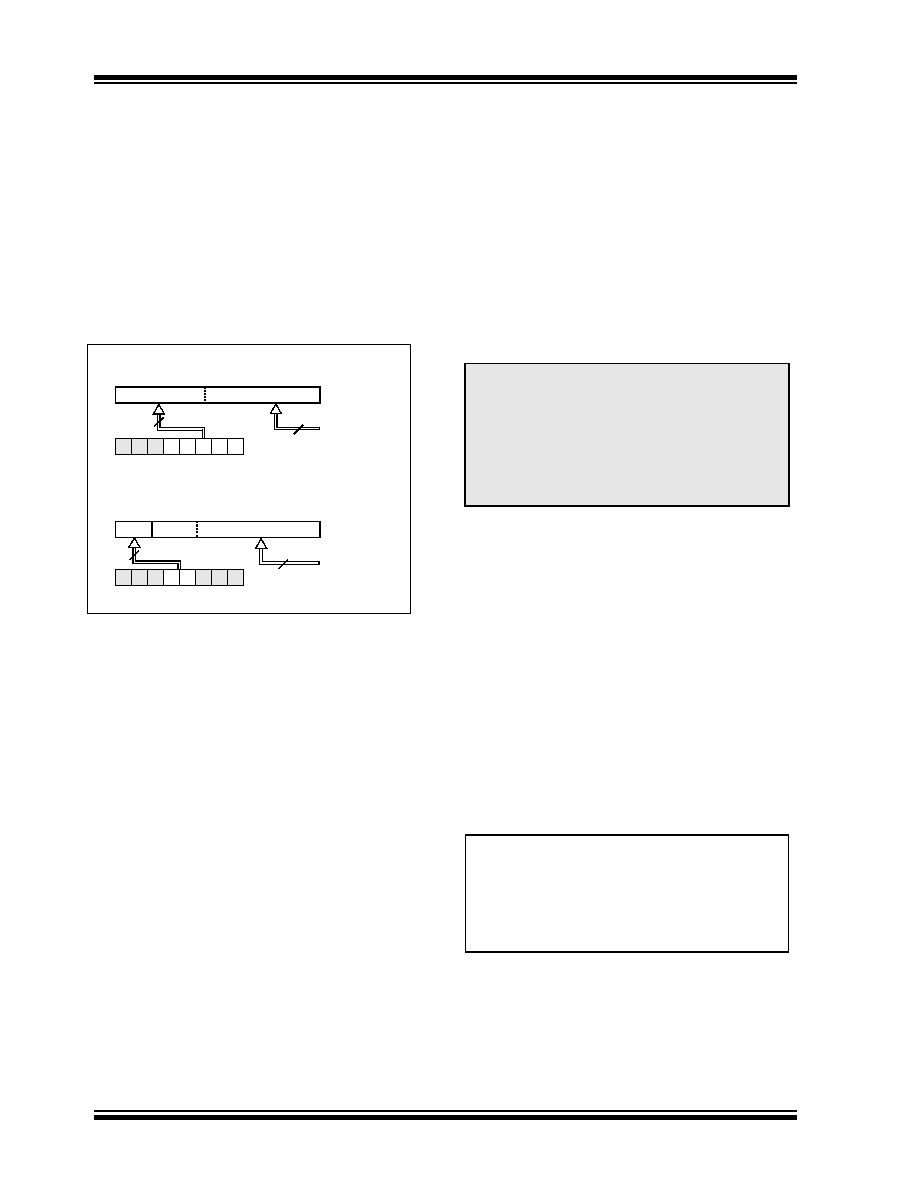
The Program Counter (PC) is 13 bits wide. The low byte
comes from the PCL register, which is a readable and
writable register. The high byte (PC<12:8>) is not directly
readable or writable and comes from PCLATH. On any
Reset, the PC is cleared. Figure 2-5 shows the two
situations for the loading of the PC. The upper example
in Figure 2-5 shows how the PC is loaded on a write to
PCL (PCLATH<4:0>
→ PCH). The lower example in
Figure 2-5 shows how the PC is loaded during a CALL or
GOTO
instruction (PCLATH<4:3>
→ PCH).
FIGURE 2-5:
LOADING OF PC IN
DIFFERENT SITUATIONS
2.3.1
MODIFYING PCL
Executing any instruction with the PCL register as the
destination
simultaneously
causes
the
Program
Counter PC<12:8> bits (PCH) to be replaced by the
contents of the PCLATH register. This allows the entire
contents of the program counter to be changed by
writing the desired upper 5 bits to the PCLATH register.
When the lower 8 bits are written to the PCL register,
all 13 bits of the program counter will change to the
values contained in the PCLATH register and those
being written to the PCL register.
A computed GOTO is accomplished by adding an offset
to the program counter (ADDWF PCL). Care should be
exercised when jumping into a look-up table or
program branch table (computed GOTO) by modifying
the PCL register. Assuming that PCLATH is set to the
table start address, if the table length is greater than
255 instructions or if the lower 8 bits of the memory
address rolls over from 0xFF to 0x00 in the middle of
the table, then PCLATH must be incremented for each
address rollover that occurs between the table
beginning and the target location within the table.
For more information refer to Application Note AN556,
“Implementing a Table Read” (DS00556).
2.3.2
STACK
The PIC16F610/616/16HV610/616 Family has an
8-level x 13-bit wide hardware stack (see Figure 2-1).
The stack space is not part of either program or data
space and the Stack Pointer is not readable or writable.
The PC is PUSHed onto the stack when a CALL
instruction is executed or an interrupt causes a branch.
The stack is POPed in the event of a RETURN, RETLW
or a RETFIE instruction execution. PCLATH is not
affected by a PUSH or POP operation.
The stack operates as a circular buffer. This means that
after the stack has been PUSHed eight times, the ninth
push overwrites the value that was stored from the first
push. The tenth push overwrites the second push (and
so on).
2.4
Indirect Addressing, INDF and
FSR Registers
The INDF register is not a physical register. Addressing
the INDF register will cause indirect addressing.
Indirect addressing is possible by using the INDF
register. Any instruction using the INDF register
actually accesses data pointed to by the File Select
Register (FSR). Reading INDF itself indirectly will
produce 00h. Writing to the INDF register indirectly
results in a no operation (although Status bits may be
affected). An effective 9-bit address is obtained by
concatenating the 8-bit FSR and the IRP bit of the
STATUS register, as shown in Figure 2-7.
A simple program to clear RAM location 40h-4Fh using
indirect addressing is shown in Example 2-1.
EXAMPLE 2-1:
INDIRECT ADDRESSING
PC
12
8
7
0
5
PCLATH<4:0>
PCLATH
Instruction with
ALU Result
GOTO, CALL
OPCODE <10:0>
8
PC
12
11 10
0
11
PCLATH<4:3>
PCH
PCL
87
2
PCLATH
PCH
PCL
PCL as
Destination
Note 1: There are no Status bits to indicate stack
overflow or stack underflow conditions.
2: There are no instructions/mnemonics
called PUSH or POP. These are actions
that occur from the execution of the
CALL,
RETURN,
RETLW
and RETFIE
instructions
or
the
vectoring
to
an
interrupt address.
MOVLW
0x40
;initialize pointer
MOVWF
FSR
;to RAM
NEXT
CLRF
INDF
;clear INDF register
INCF
FSR, F
;inc pointer
BTFSS
FSR,4
;all done?
GOTO
NEXT
;no clear next
CONTINUE
;yes continue
相关PDF资料 |
PDF描述 |
|---|---|
| PIC16LF720-I/SS | MCU PIC 2K FLASH 20-SSOP |
| PIC16F720-I/SS | MCU PIC 2K FLASH 20-SSOP |
| PIC16F526-E/P | IC PIC MCU FLASH 1KX12 14DIP |
| PIC16F610-I/P | IC PIC MCU FLASH 1KX14 14DIP |
| VE-B4N-IX-F3 | CONVERTER MOD DC/DC 18.5V 75W |
相关代理商/技术参数 |
参数描述 |
|---|---|
| PIC16HV610T-I/ML | 功能描述:8位微控制器 -MCU 1.75KB Flash 72B RAM RoHS:否 制造商:Silicon Labs 核心:8051 处理器系列:C8051F39x 数据总线宽度:8 bit 最大时钟频率:50 MHz 程序存储器大小:16 KB 数据 RAM 大小:1 KB 片上 ADC:Yes 工作电源电压:1.8 V to 3.6 V 工作温度范围:- 40 C to + 105 C 封装 / 箱体:QFN-20 安装风格:SMD/SMT |
| PIC16HV610T-I/SL | 功能描述:8位微控制器 -MCU 1.75KB Flash 72B RAM RoHS:否 制造商:Silicon Labs 核心:8051 处理器系列:C8051F39x 数据总线宽度:8 bit 最大时钟频率:50 MHz 程序存储器大小:16 KB 数据 RAM 大小:1 KB 片上 ADC:Yes 工作电源电压:1.8 V to 3.6 V 工作温度范围:- 40 C to + 105 C 封装 / 箱体:QFN-20 安装风格:SMD/SMT |
| PIC16HV610T-I/ST | 功能描述:8位微控制器 -MCU 1.75KB Flash 72B RAM RoHS:否 制造商:Silicon Labs 核心:8051 处理器系列:C8051F39x 数据总线宽度:8 bit 最大时钟频率:50 MHz 程序存储器大小:16 KB 数据 RAM 大小:1 KB 片上 ADC:Yes 工作电源电压:1.8 V to 3.6 V 工作温度范围:- 40 C to + 105 C 封装 / 箱体:QFN-20 安装风格:SMD/SMT |
| PIC16HV616-E/ML | 功能描述:8位微控制器 -MCU 4KB Flash 128 RAM RoHS:否 制造商:Silicon Labs 核心:8051 处理器系列:C8051F39x 数据总线宽度:8 bit 最大时钟频率:50 MHz 程序存储器大小:16 KB 数据 RAM 大小:1 KB 片上 ADC:Yes 工作电源电压:1.8 V to 3.6 V 工作温度范围:- 40 C to + 105 C 封装 / 箱体:QFN-20 安装风格:SMD/SMT |
| PIC16HV616-E/P | 功能描述:8位微控制器 -MCU 4KB Flash 128 RAM RoHS:否 制造商:Silicon Labs 核心:8051 处理器系列:C8051F39x 数据总线宽度:8 bit 最大时钟频率:50 MHz 程序存储器大小:16 KB 数据 RAM 大小:1 KB 片上 ADC:Yes 工作电源电压:1.8 V to 3.6 V 工作温度范围:- 40 C to + 105 C 封装 / 箱体:QFN-20 安装风格:SMD/SMT |
发布紧急采购,3分钟左右您将得到回复。