- 您现在的位置:买卖IC网 > PDF目录11463 > PIC16LC554-04I/P (Microchip Technology)IC MCU OTP 512X14 18DIP PDF资料下载
参数资料
| 型号: | PIC16LC554-04I/P |
| 厂商: | Microchip Technology |
| 文件页数: | 56/108页 |
| 文件大小: | 0K |
| 描述: | IC MCU OTP 512X14 18DIP |
| 产品培训模块: | Asynchronous Stimulus |
| 标准包装: | 25 |
| 系列: | PIC® 16C |
| 核心处理器: | PIC |
| 芯体尺寸: | 8-位 |
| 速度: | 4MHz |
| 外围设备: | POR,WDT |
| 输入/输出数: | 13 |
| 程序存储器容量: | 896B(512 x 14) |
| 程序存储器类型: | OTP |
| RAM 容量: | 80 x 8 |
| 电压 - 电源 (Vcc/Vdd): | 2.5 V ~ 5.5 V |
| 振荡器型: | 外部 |
| 工作温度: | -40°C ~ 85°C |
| 封装/外壳: | 18-DIP(0.300",7.62mm) |
| 包装: | 管件 |
第1页第2页第3页第4页第5页第6页第7页第8页第9页第10页第11页第12页第13页第14页第15页第16页第17页第18页第19页第20页第21页第22页第23页第24页第25页第26页第27页第28页第29页第30页第31页第32页第33页第34页第35页第36页第37页第38页第39页第40页第41页第42页第43页第44页第45页第46页第47页第48页第49页第50页第51页第52页第53页第54页第55页当前第56页第57页第58页第59页第60页第61页第62页第63页第64页第65页第66页第67页第68页第69页第70页第71页第72页第73页第74页第75页第76页第77页第78页第79页第80页第81页第82页第83页第84页第85页第86页第87页第88页第89页第90页第91页第92页第93页第94页第95页第96页第97页第98页第99页第100页第101页第102页第103页第104页第105页第106页第107页第108页
2002 Microchip Technology Inc.
Preliminary
DS40143D-page 49
PIC16C55X
7.2
Using Timer0 with External Clock
When an external clock input is used for Timer0, it must
meet
certain
requirements.
The
external
clock
requirement is due to internal phase clock (T
OSC)
synchronization. Also, there is a delay in the actual
incrementing of Timer0 after synchronization.
7.2.1
EXTERNAL CLOCK
SYNCHRONIZATION
When no prescaler is used, the external clock input is
the same as the prescaler output. The synchronization
of
T0CKI
with
the
internal
phase
clocks
is
accomplished by sampling the prescaler output on the
Q2 and Q4 cycles of the internal phase clocks
(Figure 7-5). Therefore, it is necessary for T0CKI to be
high for at least 2T
OSC (and a small RC delay of 20 ns)
and low for at least 2T
OSC (and a small RC delay of
20 ns). Refer to the electrical specification of the
desired device.
When a prescaler is used, the external clock input is
divided by the asynchronous ripple-counter type
prescaler so that the prescaler output is symmetrical.
For
the
external
clock
to
meet
the
sampling
requirement, the ripple-counter must be taken into
account. Therefore, it is necessary for T0CKI to have a
period of at least 4T
OSC (and a small RC delay of 40 ns)
divided by the prescaler value. The only requirement
on T0CKI high and low time is that they do not violate
the minimum pulse width requirement of 10 ns. Refer to
parameters 40, 41 and 42 in the electrical specification
of the desired device.
7.2.2
TIMER0 INCREMENT DELAY
Since the prescaler output is synchronized with the
internal clocks, there is a small delay from the time the
external clock edge occurs to the time the TMR0 is
actually incremented. Figure 7-5 shows the delay from
the external clock edge to the timer incrementing.
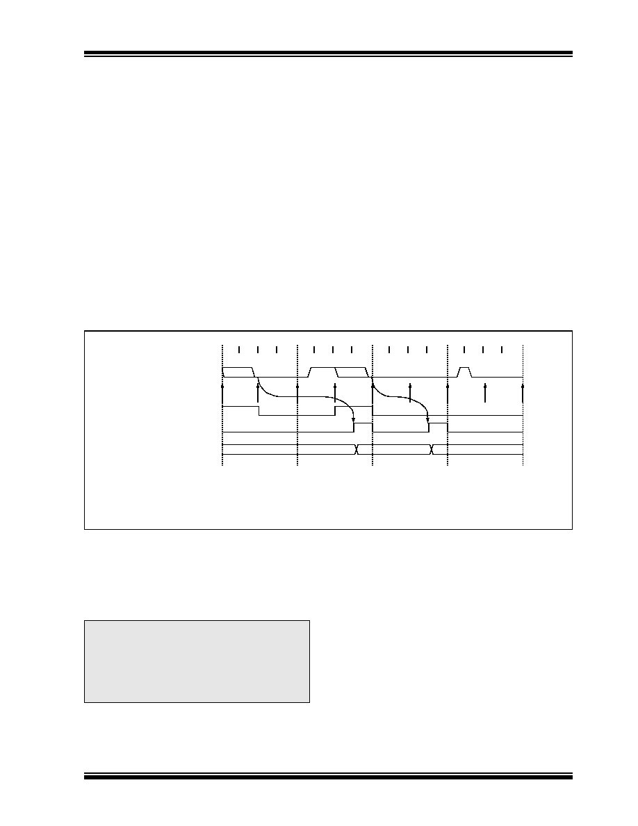
FIGURE 7-5:
TIMER0 TIMING WITH EXTERNAL CLOCK
7.3
Prescaler
An 8-bit counter is available as a prescaler for the
Timer0 module, or as a postscaler for the Watchdog
Timer, respectively (Figure 7-6). For simplicity, this
counter is being referred to as “prescaler” throughout
this data sheet.
The PSA and PS2:PS0 bits (OPTION<3:0>) determine
the prescaler assignment and prescale ratio.
When assigned to the Timer0 module, all instructions
writing
to
the
TMR0
register
(e.g.,
CLRF 1,
MOVWF 1,
BSF 1,x
....etc.) will clear the prescaler.
When assigned to WDT, a CLRWDT instruction will clear
the prescaler along with the Watchdog Timer. The
prescaler is not readable or writable.
Q1
Q2
Q3 Q4
Q1
Q2
Q3 Q4
Q1
Q2
Q3 Q4
Q1 Q2
Q3 Q4
External Clock Input or
Prescaler output (2)
External Clock/Prescaler
Output after sampling
Increment Timer0 (Q4)
Timer0
T0
T0 + 1
T0 + 2
Small pulse
misses sampling
(3)
(1)
Note
1: Delay from clock input change to Timer0 increment is 3 T
OSC to 7 TOSC. (Duration of Q = TOSC).
Therefore, the error in measuring the interval between two edges on Timer0 input = ±4 T
OSC max.
2: External clock if no prescaler selected, prescaler output otherwise.
3: The arrows indicate the points in time where sampling occurs.
Note:
There is only one prescaler available
which is mutually exclusive between the
Timer0 module and the Watchdog Timer.
Thus, a prescaler assignment for the
Timer0 module means that there is no
prescaler for the Watchdog Timer, and
vice-versa.
相关PDF资料 |
PDF描述 |
|---|---|
| VI-JWP-IY-B1 | CONVERTER MOD DC/DC 13.8V 50W |
| GRM2165C1H300GZ01D | CAP CER 30PF 50V 2% NP0 0805 |
| VI-JWN-IY-B1 | CONVERTER MOD DC/DC 18.5V 50W |
| PIC18F6310T-I/PT | IC PIC MCU FLASH 4KX16 64TQFP |
| PIC18LF1320T-I/ML | IC MCU FLASH 4KX16 EEPROM 28QFN |
相关代理商/技术参数 |
参数描述 |
|---|---|
| PIC16LC554T-04/SO | 功能描述:8位微控制器 -MCU .875KB 80 RAM 13 I/O RoHS:否 制造商:Silicon Labs 核心:8051 处理器系列:C8051F39x 数据总线宽度:8 bit 最大时钟频率:50 MHz 程序存储器大小:16 KB 数据 RAM 大小:1 KB 片上 ADC:Yes 工作电源电压:1.8 V to 3.6 V 工作温度范围:- 40 C to + 105 C 封装 / 箱体:QFN-20 安装风格:SMD/SMT |
| PIC16LC554T-04/SS | 功能描述:8位微控制器 -MCU .875KB 80 RAM 13 I/O RoHS:否 制造商:Silicon Labs 核心:8051 处理器系列:C8051F39x 数据总线宽度:8 bit 最大时钟频率:50 MHz 程序存储器大小:16 KB 数据 RAM 大小:1 KB 片上 ADC:Yes 工作电源电压:1.8 V to 3.6 V 工作温度范围:- 40 C to + 105 C 封装 / 箱体:QFN-20 安装风格:SMD/SMT |
| PIC16LC554T-04E/SO | 功能描述:8位微控制器 -MCU .875KB 80 RAM 13 I/O RoHS:否 制造商:Silicon Labs 核心:8051 处理器系列:C8051F39x 数据总线宽度:8 bit 最大时钟频率:50 MHz 程序存储器大小:16 KB 数据 RAM 大小:1 KB 片上 ADC:Yes 工作电源电压:1.8 V to 3.6 V 工作温度范围:- 40 C to + 105 C 封装 / 箱体:QFN-20 安装风格:SMD/SMT |
| PIC16LC554T-04E/SS | 功能描述:8位微控制器 -MCU .875KB 80 RAM 13 I/O RoHS:否 制造商:Silicon Labs 核心:8051 处理器系列:C8051F39x 数据总线宽度:8 bit 最大时钟频率:50 MHz 程序存储器大小:16 KB 数据 RAM 大小:1 KB 片上 ADC:Yes 工作电源电压:1.8 V to 3.6 V 工作温度范围:- 40 C to + 105 C 封装 / 箱体:QFN-20 安装风格:SMD/SMT |
| PIC16LC554T-04I/SO | 功能描述:8位微控制器 -MCU .875KB 80 RAM 13 I/O RoHS:否 制造商:Silicon Labs 核心:8051 处理器系列:C8051F39x 数据总线宽度:8 bit 最大时钟频率:50 MHz 程序存储器大小:16 KB 数据 RAM 大小:1 KB 片上 ADC:Yes 工作电源电压:1.8 V to 3.6 V 工作温度范围:- 40 C to + 105 C 封装 / 箱体:QFN-20 安装风格:SMD/SMT |
发布紧急采购,3分钟左右您将得到回复。