- 您现在的位置:买卖IC网 > PDF目录10858 > PIC16LC63AT-04/SS (Microchip Technology)IC MCU OTP 4KX14 PWM 28SSOP PDF资料下载
参数资料
| 型号: | PIC16LC63AT-04/SS |
| 厂商: | Microchip Technology |
| 文件页数: | 116/184页 |
| 文件大小: | 0K |
| 描述: | IC MCU OTP 4KX14 PWM 28SSOP |
| 标准包装: | 2,100 |
| 系列: | PIC® 16C |
| 核心处理器: | PIC |
| 芯体尺寸: | 8-位 |
| 速度: | 4MHz |
| 连通性: | I²C,SPI,UART/USART |
| 外围设备: | 欠压检测/复位,POR,PWM,WDT |
| 输入/输出数: | 22 |
| 程序存储器容量: | 7KB(4K x 14) |
| 程序存储器类型: | OTP |
| RAM 容量: | 192 x 8 |
| 电压 - 电源 (Vcc/Vdd): | 2.5 V ~ 5.5 V |
| 振荡器型: | 外部 |
| 工作温度: | 0°C ~ 70°C |
| 封装/外壳: | 28-SSOP(0.209",5.30mm 宽) |
| 包装: | 带卷 (TR) |
第1页第2页第3页第4页第5页第6页第7页第8页第9页第10页第11页第12页第13页第14页第15页第16页第17页第18页第19页第20页第21页第22页第23页第24页第25页第26页第27页第28页第29页第30页第31页第32页第33页第34页第35页第36页第37页第38页第39页第40页第41页第42页第43页第44页第45页第46页第47页第48页第49页第50页第51页第52页第53页第54页第55页第56页第57页第58页第59页第60页第61页第62页第63页第64页第65页第66页第67页第68页第69页第70页第71页第72页第73页第74页第75页第76页第77页第78页第79页第80页第81页第82页第83页第84页第85页第86页第87页第88页第89页第90页第91页第92页第93页第94页第95页第96页第97页第98页第99页第100页第101页第102页第103页第104页第105页第106页第107页第108页第109页第110页第111页第112页第113页第114页第115页当前第116页第117页第118页第119页第120页第121页第122页第123页第124页第125页第126页第127页第128页第129页第130页第131页第132页第133页第134页第135页第136页第137页第138页第139页第140页第141页第142页第143页第144页第145页第146页第147页第148页第149页第150页第151页第152页第153页第154页第155页第156页第157页第158页第159页第160页第161页第162页第163页第164页第165页第166页第167页第168页第169页第170页第171页第172页第173页第174页第175页第176页第177页第178页第179页第180页第181页第182页第183页第184页
2000 Microchip Technology Inc.
DS30605C-page 37
PIC16C63A/65B/73B/74B
5.6
Parallel Slave Port (PSP)
PORTD operates as an 8-bit wide Parallel Slave Port
(PSP), or microprocessor port when control bit PSP-
MODE (TRISE<4>) is set. In Slave mode, it is asyn-
chronously readable and writable by the external world,
through RD control input pin RE0/RD/AN5 and WR
control input pin RE1/WR/AN6.
It can directly interface to an 8-bit microprocessor data
bus. The external microprocessor can read or write the
PORTD latch as an 8-bit latch. Setting bit PSPMODE
enables port pin RE0/RD/AN5 to be the RD input,
RE1/WR/AN6 to be the WR input and RE2/CS/AN7 to
be the CS (chip select) input. For this functionality, the
corresponding data direction bits of the TRISE register
(TRISE<2:0>) must be configured as inputs (set) and
the
A/D
port
configuration
bits
PCFG2:PCFG0
(ADCON1<2:0>) must be set, which will configure pins
RE2:RE0 as digital I/O.
There are actually two 8-bit latches, one for data out
(from the PICmicro MCU) and one for data input. The
user writes 8-bit data to PORTD data latch and reads
data from the port pin latch (note that they have the
same address). In this mode, the TRISD register is
ignored since the external device is controlling the
direction of data flow.
A write to the PSP occurs when both the CS and WR
lines are first detected low. When either the CS or WR
lines become high (level triggered), then the Input
Buffer Full (IBF) status flag bit (TRISE<7>) is set on the
Q4 clock cycle, following the next Q2 cycle, to signal
the write is complete (Figure 5-9). The interrupt flag bit
PSPIF (PIR1<7>) is also set on the same Q4 clock
cycle. IBF can only be cleared by reading the PORTD
input latch. The Input Buffer Overflow (IBOV) status
flag bit (TRISE<5>) is set if a second write to the PSP
is attempted when the previous byte has not been read
out of the buffer.
A read from the PSP occurs when both the CS and RD
lines are first detected low. The Output Buffer Full
(OBF) status flag bit (TRISE<6>) is cleared immedi-
ately (Figure 5-10), indicating that the PORTD latch is
waiting to be read by the external bus. When either the
CS or RD pin becomes high (level triggered), the inter-
rupt flag bit PSPIF is set on the Q4 clock cycle, follow-
ing the next Q2 cycle, indicating that the read is
complete. OBF remains low until data is written to
PORTD by the user firmware.
When not in PSP mode, the IBF and OBF bits are held
clear. However, if flag bit IBOV was previously set, it
must be cleared in firmware.
An interrupt is generated and latched into flag bit
PSPIF when a read or write operation is completed.
PSPIF must be cleared by the user in firmware and the
interrupt can be disabled by clearing the interrupt
enable bit PSPIE (PIE1<7>).
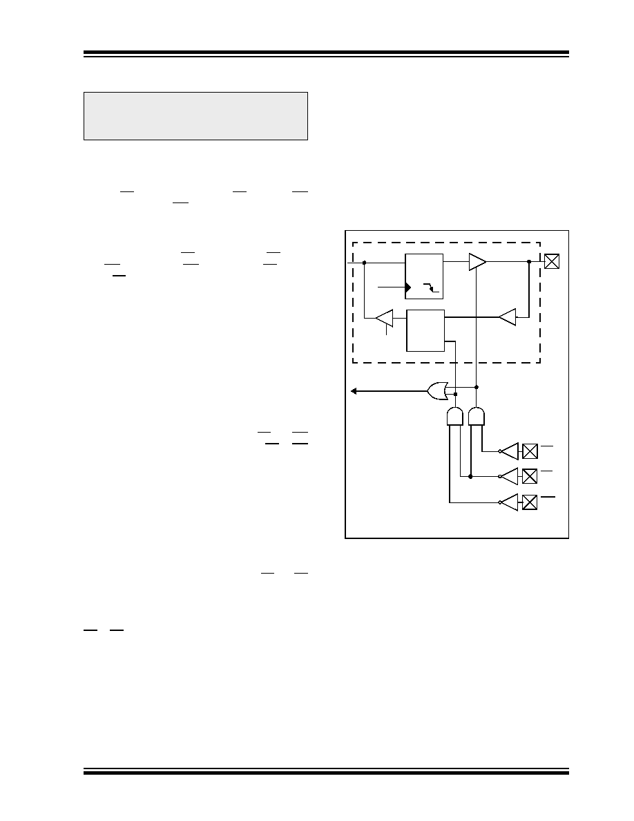
FIGURE 5-8:
PORTD AND PORTE
BLOCK DIAGRAM
(PARALLEL SLAVE
PORT)
Note:
The PIC16C63A and PIC16C73B do not
provide a parallel slave port. The PORTD,
PORTE, TRISD and TRISE registers are
not implemented.
Data Bus
WR
Port
RD
RDx
Q
D
CK
EN
QD
EN
Port
pin
One bit of PORTD
Set Interrupt Flag
PSPIF (PIR1<7>)
Read
Chip Select
Write
RD
CS
WR
TTL
Note 1: I/O pins have protection diodes to VDD and VSS.
相关PDF资料 |
PDF描述 |
|---|---|
| PIC16LC63AT-04/SO | IC MCU OTP 4KX14 PWM 28SOIC |
| PIC16LC62BT-04/SS | IC MCU OTP 2KX14 PWM 28SSOP |
| PIC16LC62BT-04I/SO | IC MCU OTP 2KX14 PWM 28SOIC |
| PIC16LC62AT-04/SS | IC MCU OTP 2KX14 PWM 28SSOP |
| PIC16LC62AT-04/SO | IC MCU OTP 2KX14 PWM 28SOIC |
相关代理商/技术参数 |
参数描述 |
|---|---|
| PIC16LC63T-04/SO | 功能描述:8位微控制器 -MCU 7KB 192 RAM 22 I/O RoHS:否 制造商:Silicon Labs 核心:8051 处理器系列:C8051F39x 数据总线宽度:8 bit 最大时钟频率:50 MHz 程序存储器大小:16 KB 数据 RAM 大小:1 KB 片上 ADC:Yes 工作电源电压:1.8 V to 3.6 V 工作温度范围:- 40 C to + 105 C 封装 / 箱体:QFN-20 安装风格:SMD/SMT |
| PIC16LC63T-04I/SO | 功能描述:8位微控制器 -MCU 7KB 192 RAM 22 I/O RoHS:否 制造商:Silicon Labs 核心:8051 处理器系列:C8051F39x 数据总线宽度:8 bit 最大时钟频率:50 MHz 程序存储器大小:16 KB 数据 RAM 大小:1 KB 片上 ADC:Yes 工作电源电压:1.8 V to 3.6 V 工作温度范围:- 40 C to + 105 C 封装 / 箱体:QFN-20 安装风格:SMD/SMT |
| PIC16LC64041P | 制造商:MICHIP 功能描述: |
| PIC16LC642-04/SO | 功能描述:8位微控制器 -MCU 7KB 176 RAM 22 I/O RoHS:否 制造商:Silicon Labs 核心:8051 处理器系列:C8051F39x 数据总线宽度:8 bit 最大时钟频率:50 MHz 程序存储器大小:16 KB 数据 RAM 大小:1 KB 片上 ADC:Yes 工作电源电压:1.8 V to 3.6 V 工作温度范围:- 40 C to + 105 C 封装 / 箱体:QFN-20 安装风格:SMD/SMT |
| PIC16LC642-04/SP | 功能描述:8位微控制器 -MCU 7KB 176 RAM 22 I/O RoHS:否 制造商:Silicon Labs 核心:8051 处理器系列:C8051F39x 数据总线宽度:8 bit 最大时钟频率:50 MHz 程序存储器大小:16 KB 数据 RAM 大小:1 KB 片上 ADC:Yes 工作电源电压:1.8 V to 3.6 V 工作温度范围:- 40 C to + 105 C 封装 / 箱体:QFN-20 安装风格:SMD/SMT |
发布紧急采购,3分钟左右您将得到回复。