- 您现在的位置:买卖IC网 > PDF目录3883 > PIC16LC63AT-04I/ML (Microchip Technology)IC MCU OTP 4KX14 LV 28-QFN PDF资料下载
参数资料
| 型号: | PIC16LC63AT-04I/ML |
| 厂商: | Microchip Technology |
| 文件页数: | 107/184页 |
| 文件大小: | 0K |
| 描述: | IC MCU OTP 4KX14 LV 28-QFN |
| 标准包装: | 1,600 |
| 系列: | PIC® 16C |
| 核心处理器: | PIC |
| 芯体尺寸: | 8-位 |
| 速度: | 4MHz |
| 连通性: | I²C,SPI,UART/USART |
| 外围设备: | 欠压检测/复位,POR,PWM,WDT |
| 输入/输出数: | 22 |
| 程序存储器容量: | 7KB(4K x 14) |
| 程序存储器类型: | OTP |
| RAM 容量: | 192 x 8 |
| 电压 - 电源 (Vcc/Vdd): | 2.5 V ~ 5.5 V |
| 振荡器型: | 外部 |
| 工作温度: | -40°C ~ 85°C |
| 封装/外壳: | 28-VQFN 裸露焊盘 |
| 包装: | 带卷 (TR) |
| 其它名称: | PIC16LC63AT04I/ML |
第1页第2页第3页第4页第5页第6页第7页第8页第9页第10页第11页第12页第13页第14页第15页第16页第17页第18页第19页第20页第21页第22页第23页第24页第25页第26页第27页第28页第29页第30页第31页第32页第33页第34页第35页第36页第37页第38页第39页第40页第41页第42页第43页第44页第45页第46页第47页第48页第49页第50页第51页第52页第53页第54页第55页第56页第57页第58页第59页第60页第61页第62页第63页第64页第65页第66页第67页第68页第69页第70页第71页第72页第73页第74页第75页第76页第77页第78页第79页第80页第81页第82页第83页第84页第85页第86页第87页第88页第89页第90页第91页第92页第93页第94页第95页第96页第97页第98页第99页第100页第101页第102页第103页第104页第105页第106页当前第107页第108页第109页第110页第111页第112页第113页第114页第115页第116页第117页第118页第119页第120页第121页第122页第123页第124页第125页第126页第127页第128页第129页第130页第131页第132页第133页第134页第135页第136页第137页第138页第139页第140页第141页第142页第143页第144页第145页第146页第147页第148页第149页第150页第151页第152页第153页第154页第155页第156页第157页第158页第159页第160页第161页第162页第163页第164页第165页第166页第167页第168页第169页第170页第171页第172页第173页第174页第175页第176页第177页第178页第179页第180页第181页第182页第183页第184页
2000 Microchip Technology Inc.
DS30605C-page 29
PIC16C63A/65B/73B/74B
5.0
I/O PORTS
Some pins for these I/O ports are multiplexed with an
alternate function for the peripheral features on the
device. In general, when a peripheral is enabled, that
pin may not be used as a general purpose I/O pin.
5.1
PORTA and TRISA Registers
PORTA is a 6-bit latch.
The RA4/T0CKI pin is a Schmitt Trigger input and an
open drain output. All other RA port pins have TTL
input levels and full CMOS output drivers. All pins have
data direction bits (TRIS registers), which can config-
ure these pins as output or input.
Setting a TRISA register bit puts the corresponding out-
put driver in a hi-impedance mode. Clearing a bit in the
TRISA register puts the contents of the output latch on
the selected pin(s).
Reading the PORTA register reads the status of the
pins, whereas writing to it will write to the port latch. All
write operations are read-modify-write operations.
Therefore, a write to a port implies that the port pins are
read, the value is modified and then written to the port
data latch.
Pin RA4 is multiplexed with the Timer0 module clock
input to become the RA4/T0CKI pin.
On the PIC16C73B/74B, PORTA pins are multiplexed
with analog inputs and analog VREF input. The opera-
tion of each pin is selected by clearing/setting the con-
trol bits in the ADCON1 register (A/D Control
Register1).
The TRISA register controls the direction of the RA
pins, even when they are being used as analog inputs.
The user must ensure the bits in the TRISA register are
maintained set when using them as analog inputs.
EXAMPLE 5-1:
INITIALIZING PORTA
(PIC16C73B/74B)
BCF
STATUS, RP0
;
CLRF
PORTA
; Initialize PORTA by
; clearing output
; data latches
BSF
STATUS, RP0
; Select Bank 1
MOVLW
0x06
; Configure all pins
MOVWF
ADCON1
; as digital inputs
MOVLW
0xCF
; Value used to
; initialize data
; direction
MOVWF
TRISA
; Set RA<3:0> as inputs
; RA<5:4> as outputs
; TRISA<7:6> are always
; read as ’0’.
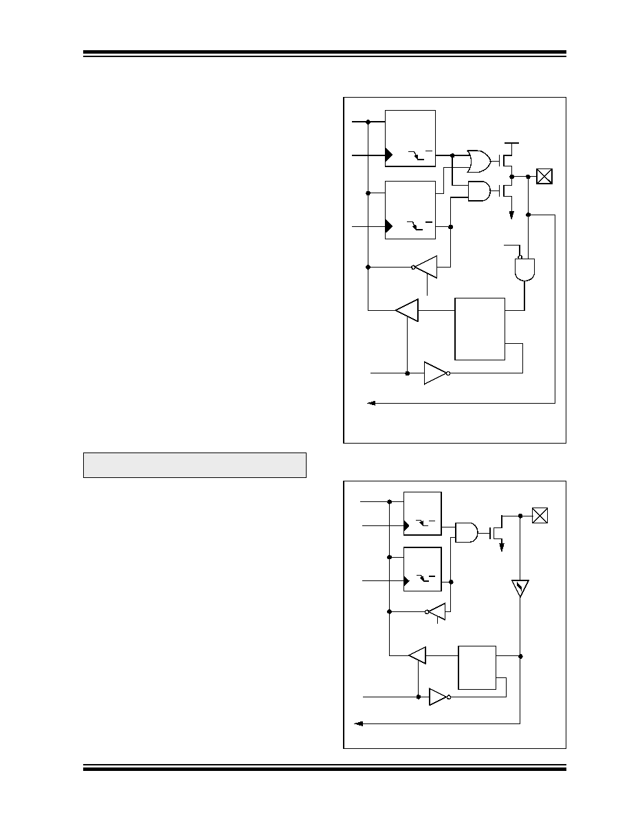
FIGURE 5-1:
BLOCK DIAGRAM OF
RA3:RA0 AND RA5 PINS
FIGURE 5-2:
BLOCK DIAGRAM OF
RA4/T0CKI PIN
Note:
On all RESETS, pins with analog functions
are configured as analog and digital inputs.
Data
Bus
Q
D
Q
CK
Q
D
Q
CK
QD
EN
P
N
WR
Port
WR
TRIS
Data Latch
TRIS Latch
RD TRIS
RD Port
VSS
VDD
I/O pin(1)
Note
1:
I/O pins have protection diodes to VDD and VSS.
Analog
Input
mode
TTL
Input
Buffer
To A/D Converter
Data
Bus
WR
Port
WR
TRIS
RD Port
Data Latch
TRIS Latch
RD TRIS
Schmitt
Trigger
Input
Buffer
N
VSS
I/O pin
TMR0 Clock Input
Q
D
Q
CK
Q
D
Q
CK
EN
QD
EN
(1)
Note
1: I/O pins have protection diodes to VDD and VSS.
相关PDF资料 |
PDF描述 |
|---|---|
| PIC12C508-04/SM | IC MCU OTP 512X12 8-SOIJ |
| PIC16LC62BT-04I/ML | IC MCU OTP 2KX14 LV 28-QFN |
| PIC16F628T-20E/SS | IC MCU FLASH 2KX14 20-SSOP |
| PIC16F628T-04E/SS | IC MCU FLASH 2KX14 20-SSOP |
| PIC18LF248T-I/SO | IC MCU FLASH 8KX16 LV CAN 28SOIC |
相关代理商/技术参数 |
参数描述 |
|---|---|
| PIC16LC63T-04/SO | 功能描述:8位微控制器 -MCU 7KB 192 RAM 22 I/O RoHS:否 制造商:Silicon Labs 核心:8051 处理器系列:C8051F39x 数据总线宽度:8 bit 最大时钟频率:50 MHz 程序存储器大小:16 KB 数据 RAM 大小:1 KB 片上 ADC:Yes 工作电源电压:1.8 V to 3.6 V 工作温度范围:- 40 C to + 105 C 封装 / 箱体:QFN-20 安装风格:SMD/SMT |
| PIC16LC63T-04I/SO | 功能描述:8位微控制器 -MCU 7KB 192 RAM 22 I/O RoHS:否 制造商:Silicon Labs 核心:8051 处理器系列:C8051F39x 数据总线宽度:8 bit 最大时钟频率:50 MHz 程序存储器大小:16 KB 数据 RAM 大小:1 KB 片上 ADC:Yes 工作电源电压:1.8 V to 3.6 V 工作温度范围:- 40 C to + 105 C 封装 / 箱体:QFN-20 安装风格:SMD/SMT |
| PIC16LC64041P | 制造商:MICHIP 功能描述: |
| PIC16LC642-04/SO | 功能描述:8位微控制器 -MCU 7KB 176 RAM 22 I/O RoHS:否 制造商:Silicon Labs 核心:8051 处理器系列:C8051F39x 数据总线宽度:8 bit 最大时钟频率:50 MHz 程序存储器大小:16 KB 数据 RAM 大小:1 KB 片上 ADC:Yes 工作电源电压:1.8 V to 3.6 V 工作温度范围:- 40 C to + 105 C 封装 / 箱体:QFN-20 安装风格:SMD/SMT |
| PIC16LC642-04/SP | 功能描述:8位微控制器 -MCU 7KB 176 RAM 22 I/O RoHS:否 制造商:Silicon Labs 核心:8051 处理器系列:C8051F39x 数据总线宽度:8 bit 最大时钟频率:50 MHz 程序存储器大小:16 KB 数据 RAM 大小:1 KB 片上 ADC:Yes 工作电源电压:1.8 V to 3.6 V 工作温度范围:- 40 C to + 105 C 封装 / 箱体:QFN-20 安装风格:SMD/SMT |
发布紧急采购,3分钟左右您将得到回复。