- 您现在的位置:买卖IC网 > PDF目录10857 > PIC16LC65AT-04I/PQ (Microchip Technology)IC MCU OTP 4KX14 PWM 44-MQFP PDF资料下载
参数资料
| 型号: | PIC16LC65AT-04I/PQ |
| 厂商: | Microchip Technology |
| 文件页数: | 120/126页 |
| 文件大小: | 0K |
| 描述: | IC MCU OTP 4KX14 PWM 44-MQFP |
| 标准包装: | 900 |
| 系列: | PIC® 16C |
| 核心处理器: | PIC |
| 芯体尺寸: | 8-位 |
| 速度: | 4MHz |
| 连通性: | I²C,SPI,UART/USART |
| 外围设备: | 欠压检测/复位,POR,PWM,WDT |
| 输入/输出数: | 33 |
| 程序存储器容量: | 7KB(4K x 14) |
| 程序存储器类型: | OTP |
| RAM 容量: | 192 x 8 |
| 电压 - 电源 (Vcc/Vdd): | 2.5 V ~ 6 V |
| 振荡器型: | 外部 |
| 工作温度: | -40°C ~ 85°C |
| 封装/外壳: | 44-QFP |
| 包装: | 带卷 (TR) |
| 其它名称: | PIC16LC65AT-04IPQ |
第1页第2页第3页第4页第5页第6页第7页第8页第9页第10页第11页第12页第13页第14页第15页第16页第17页第18页第19页第20页第21页第22页第23页第24页第25页第26页第27页第28页第29页第30页第31页第32页第33页第34页第35页第36页第37页第38页第39页第40页第41页第42页第43页第44页第45页第46页第47页第48页第49页第50页第51页第52页第53页第54页第55页第56页第57页第58页第59页第60页第61页第62页第63页第64页第65页第66页第67页第68页第69页第70页第71页第72页第73页第74页第75页第76页第77页第78页第79页第80页第81页第82页第83页第84页第85页第86页第87页第88页第89页第90页第91页第92页第93页第94页第95页第96页第97页第98页第99页第100页第101页第102页第103页第104页第105页第106页第107页第108页第109页第110页第111页第112页第113页第114页第115页第116页第117页第118页第119页当前第120页第121页第122页第123页第124页第125页第126页
93
AT90S/LS4433
1042H–AVR–04/03
Serial Downloading
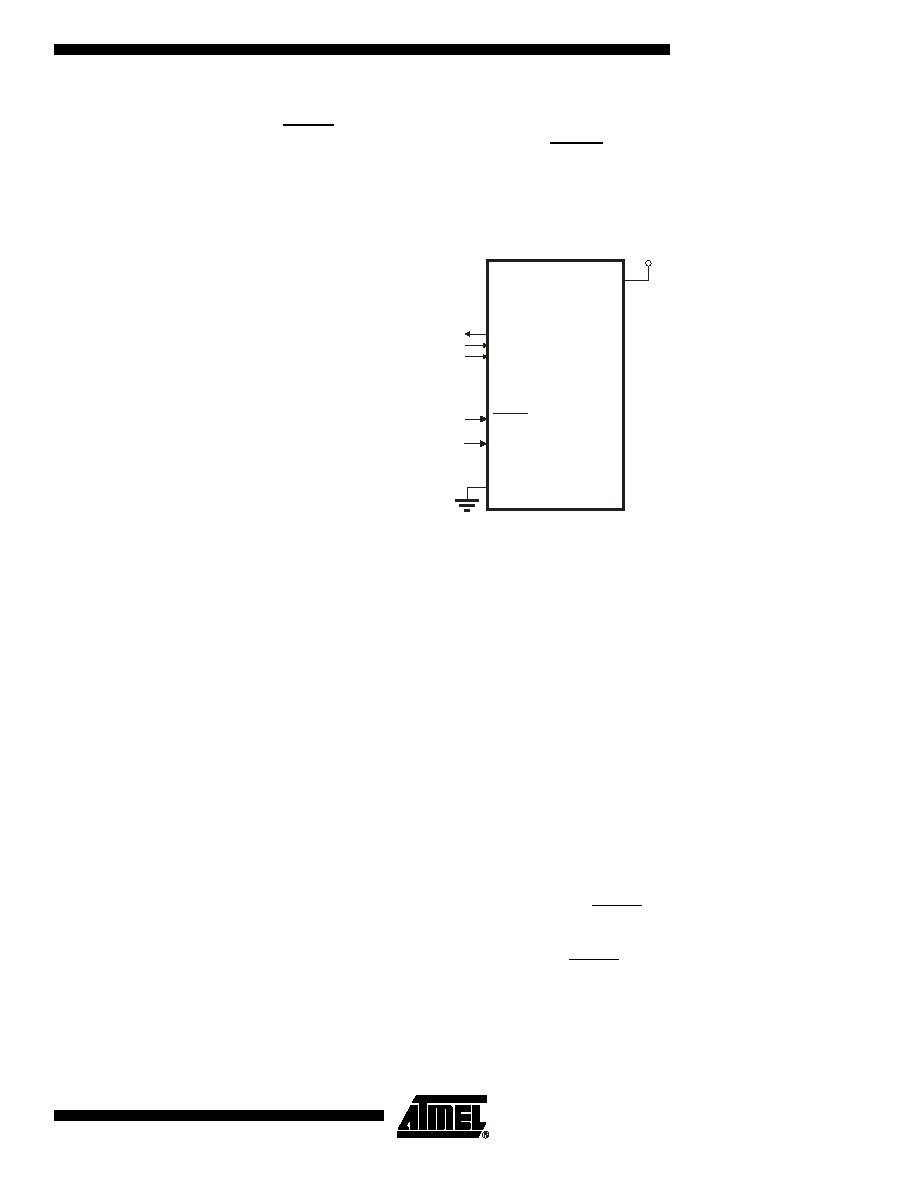
Both the Program and Data memory arrays can be programmed using the SPI bus while
RESET is pulled to GND. The serial interface consists of pins SCK, MOSI (input) and
MISO (output) (see Figure 66). After RESET is set low, the Programming Enable
instruction needs to be executed first before program/erase instructions can be
executed.
Figure 66. Serial Programming and Verify
For the EEPROM, an auto-erase cycle is provided within the self-timed write instruction
and there is no need to first execute the Chip Erase instruction. The Chip Erase instruc-
tion turns the content of every memory location in both the program and EEPROM
arrays into $FF.
The Program and EEPROM memory arrays have separate address spaces: 0000 to
$07FF for Program memory and $0000 to $00FF for EEPROM memory.
Either an external system clock is supplied at pin XTAL1 or a crystal needs to be con-
nected across pins XTAL1 and XTAL2. The minimum low and high periods for the serial
clock (SCK) input are defined as follows:
Low: > 2 XTAL1 clock cycles
High: > 2 XTAL1 clock cycles
Serial Programming
Algorithm
When writing serial data to the AT90S4433, data is clocked on the rising edge of CLK.
When reading data from the AT90S4433, data is clocked on the falling edge of CLK.
See Figure 67, Figure 68 and Table 36 for details.
To program and verify the AT90S4433 in the Serial Programming mode, the following
sequence is recommended (see 4-byte instruction formats in Table 35
):
1.
Power-up sequence:
Apply power between V
CC and GND while RESET and SCK are set to “0”. If a
crystal is not connected across pins XTAL1 and XTAL2, apply a clock signal to
the XTAL1 pin. In some systems, the programmer cannot guarantee that SCK is
held low during Power-up. In this case, RESET must be given a positive pulse of
at least two XTAL1 cycles’ duration after SCK has been set to “0”.
2.
Wait for at least 20 ms and enable serial programming by sending the Program-
ming Enable serial instruction to pin MOSI/PB3.
3.
The serial programming instructions will not work if the communication is out of
synchronization. When in sync, the second byte ($53) will echo back when issu-
AT90S/LS4433
VCC
4.0 - 6.0 V (AT90S4433)
2.7 - 6.0 V (AT90LS4433)
PB5(SCK)
PB4(MISO)
PB3(MOSI)
RESET
GND
XTAL1
CLOCK IN
GND
DATA OUT
INSTR. IN
CLOCK
INPUT
相关PDF资料 |
PDF描述 |
|---|---|
| PIC16LC65AT-04I/L | IC MCU OTP 4KX14 PWM 44PLCC |
| PIC16LC65A-04I/PT | IC MCU OTP 4KX14 PWM 44TQFP |
| VE-J5B-IX-F3 | CONVERTER MOD DC/DC 95V 75W |
| VE-J5B-IX-F2 | CONVERTER MOD DC/DC 95V 75W |
| ADN2813ACPZ-RL7 | IC CLK/DATA REC 1.25GBPS 32LFCSP |
相关代理商/技术参数 |
参数描述 |
|---|---|
| PIC16LC65B-04/L | 功能描述:8位微控制器 -MCU 7KB 192 RAM 33 I/O RoHS:否 制造商:Silicon Labs 核心:8051 处理器系列:C8051F39x 数据总线宽度:8 bit 最大时钟频率:50 MHz 程序存储器大小:16 KB 数据 RAM 大小:1 KB 片上 ADC:Yes 工作电源电压:1.8 V to 3.6 V 工作温度范围:- 40 C to + 105 C 封装 / 箱体:QFN-20 安装风格:SMD/SMT |
| PIC16LC65B-04/P | 功能描述:8位微控制器 -MCU 7KB 192 RAM 33 I/O RoHS:否 制造商:Silicon Labs 核心:8051 处理器系列:C8051F39x 数据总线宽度:8 bit 最大时钟频率:50 MHz 程序存储器大小:16 KB 数据 RAM 大小:1 KB 片上 ADC:Yes 工作电源电压:1.8 V to 3.6 V 工作温度范围:- 40 C to + 105 C 封装 / 箱体:QFN-20 安装风格:SMD/SMT |
| PIC16LC65B-04/PQ | 功能描述:8位微控制器 -MCU 7KB 192 RAM 33 I/O RoHS:否 制造商:Silicon Labs 核心:8051 处理器系列:C8051F39x 数据总线宽度:8 bit 最大时钟频率:50 MHz 程序存储器大小:16 KB 数据 RAM 大小:1 KB 片上 ADC:Yes 工作电源电压:1.8 V to 3.6 V 工作温度范围:- 40 C to + 105 C 封装 / 箱体:QFN-20 安装风格:SMD/SMT |
| PIC16LC65B-04/PT | 功能描述:8位微控制器 -MCU 7KB 192 RAM 33 I/O RoHS:否 制造商:Silicon Labs 核心:8051 处理器系列:C8051F39x 数据总线宽度:8 bit 最大时钟频率:50 MHz 程序存储器大小:16 KB 数据 RAM 大小:1 KB 片上 ADC:Yes 工作电源电压:1.8 V to 3.6 V 工作温度范围:- 40 C to + 105 C 封装 / 箱体:QFN-20 安装风格:SMD/SMT |
| PIC16LC65B-04I/L | 功能描述:8位微控制器 -MCU 7KB 192 RAM 33 I/O RoHS:否 制造商:Silicon Labs 核心:8051 处理器系列:C8051F39x 数据总线宽度:8 bit 最大时钟频率:50 MHz 程序存储器大小:16 KB 数据 RAM 大小:1 KB 片上 ADC:Yes 工作电源电压:1.8 V to 3.6 V 工作温度范围:- 40 C to + 105 C 封装 / 箱体:QFN-20 安装风格:SMD/SMT |
发布紧急采购,3分钟左右您将得到回复。