- 您现在的位置:买卖IC网 > PDF目录10856 > PIC16LC712T-04/SS (Microchip Technology)IC MCU OTP 1KX14 A/D PWM 20SSOP PDF资料下载
参数资料
| 型号: | PIC16LC712T-04/SS |
| 厂商: | Microchip Technology |
| 文件页数: | 71/106页 |
| 文件大小: | 0K |
| 描述: | IC MCU OTP 1KX14 A/D PWM 20SSOP |
| 标准包装: | 1,600 |
| 系列: | PIC® 16C |
| 核心处理器: | PIC |
| 芯体尺寸: | 8-位 |
| 速度: | 4MHz |
| 外围设备: | 欠压检测/复位,POR,PWM,WDT |
| 输入/输出数: | 13 |
| 程序存储器容量: | 1.75KB(1K x 14) |
| 程序存储器类型: | OTP |
| RAM 容量: | 128 x 8 |
| 电压 - 电源 (Vcc/Vdd): | 2.5 V ~ 5.5 V |
| 数据转换器: | A/D 4x8b |
| 振荡器型: | 外部 |
| 工作温度: | 0°C ~ 70°C |
| 封装/外壳: | 20-SSOP(0.209",5.30mm 宽) |
| 包装: | 带卷 (TR) |
第1页第2页第3页第4页第5页第6页第7页第8页第9页第10页第11页第12页第13页第14页第15页第16页第17页第18页第19页第20页第21页第22页第23页第24页第25页第26页第27页第28页第29页第30页第31页第32页第33页第34页第35页第36页第37页第38页第39页第40页第41页第42页第43页第44页第45页第46页第47页第48页第49页第50页第51页第52页第53页第54页第55页第56页第57页第58页第59页第60页第61页第62页第63页第64页第65页第66页第67页第68页第69页第70页当前第71页第72页第73页第74页第75页第76页第77页第78页第79页第80页第81页第82页第83页第84页第85页第86页第87页第88页第89页第90页第91页第92页第93页第94页第95页第96页第97页第98页第99页第100页第101页第102页第103页第104页第105页第106页
2005 Microchip Technology Inc.
DS41106B-page 65
PIC16C712/716
When the SLEEP instruction is being executed, the next
instruction (PC + 1) is pre-fetched. For the device to
wake-up through an interrupt event, the corresponding
interrupt enable bit must be set (enabled). Wake-up is
regardless of the state of the GIE bit. If the GIE bit is
clear (disabled), the device continues execution at the
instruction after the SLEEP instruction. If the GIE bit is
set (enabled), the device executes the instruction after
the SLEEP instruction and then branches to the inter-
rupt address (0004h). In cases where the execution of
the instruction following SLEEP is not desirable, the
user should have a NOP after the SLEEP instruction.
9.13.2
WAKE-UP USING INTERRUPTS
When global interrupts are disabled (GIE cleared) and
any interrupt source has both its interrupt enable bit
and interrupt flag bit set, one of the following will occur:
If the interrupt occurs before the execution of a
SLEEP
instruction, the SLEEP instruction will
complete as a NOP. Therefore, the WDT and WDT
postscaler will not be cleared, the TO bit will not
be set and PD bits will not be cleared.
If the interrupt occurs during or after the execu-
tion of a SLEEP instruction, the device will imme-
diately wake-up from Sleep. The SLEEP
instruction will be completely executed before the
wake-up. Therefore, the WDT and WDT
postscaler will be cleared, the TO bit will be set
and the PD bit will be cleared.
Even if the flag bits were checked before executing a
SLEEP
instruction, it may be possible for flag bits to
become set before the SLEEP instruction completes. To
determine whether a SLEEP instruction executed, test
the PD bit. If the PD bit is set, the SLEEP instruction
was executed as a NOP.
To ensure that the WDT is cleared, a CLRWDT instruc-
tion should be executed before a SLEEP instruction.
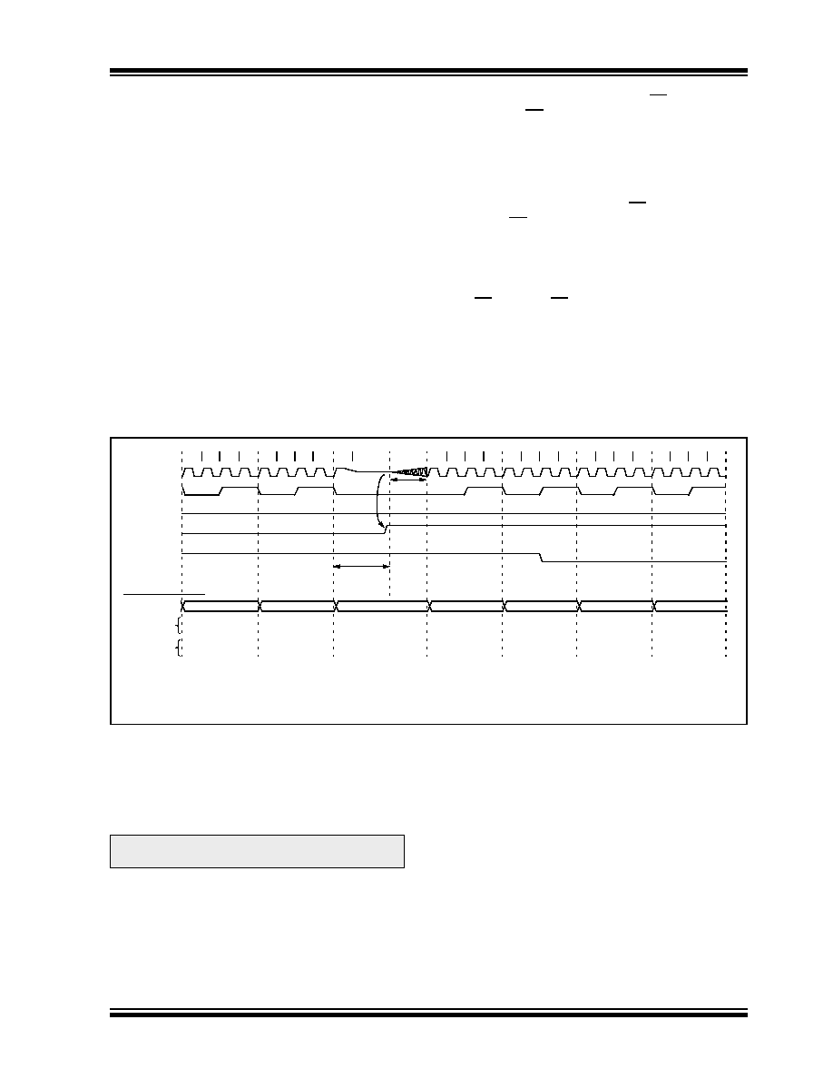
FIGURE 9-17:
WAKE-UP FROM SLEEP THROUGH INTERRUPT
9.14
Program Verification/Code
Protection
If
the
code
protection
bit(s)
have
not
been
programmed, the on-chip program memory can be
read out for verification purposes.
9.15
ID Locations
Four memory locations (2000h-2003h) are designated
as ID locations where the user can store checksum or
other code-identification numbers. These locations are
not accessible during normal execution, but are read-
able
and
writable
during
Program/Verify.
It
is
recommended that only the 4 Least Significant bits of
the ID location are used.
For ROM devices, these values are submitted along
with the ROM code.
Q1
Q2
Q3 Q4
Q1 Q2
Q3
Q4
Q1
Q2 Q3 Q4
Q1 Q2 Q3 Q4
Q1
Q2 Q3
Q4
Q1 Q2
Q3
Q4
OSC1
CLKOUT(4)
INT pin
INTF flag
(INTCON<1>)
GIE bit
(INTCON<7>)
INSTRUCTION FLOW
PC
Instruction
fetched
Instruction
executed
PC
PC + 1
PC + 2
Inst(PC) = Sleep
Inst(PC - 1)
Inst(PC + 1)
Sleep
Processor in
Sleep
Interrupt Latency
(Note 2)
Inst(PC + 2)
Inst(PC + 1)
Inst(0004h)
Inst(0005h)
Inst(0004h)
Dummy cycle
PC + 2
0004h
0005h
Dummy cycle
TOST(2)
PC + 2
Note 1:
XT, HS or LP Oscillator mode assumed.
2:
TOST = 1024TOSC (drawing not to scale) This delay will not be there for RC Osc mode.
3:
GIE = 1 assumed. In this case after wake-up, the processor jumps to the interrupt routine. If GIE = 0, execution will continue in-line.
4:
CLKOUT is not available in these osc modes, but shown here for timing reference.
Note:
Microchip does not recommend code
protecting windowed devices.
相关PDF资料 |
PDF描述 |
|---|---|
| PIC16LC712T-04I/SO | IC MCU OTP 1KX14 A/D PWM 18SOIC |
| PIC16LC711T-04E/SS | IC MCU OTP 1KX14 A/D 20SSOP |
| PIC16LC711T-04E/SO | IC MCU OTP 1KX14 A/D 18SOIC |
| PIC16LC710T-04/SS | IC MCU OTP 512X14 A/D 20SSOP |
| PIC16LC710T-04I/SS | IC MCU OTP 512X14 A/D 20SSOP |
相关代理商/技术参数 |
参数描述 |
|---|---|
| PIC16LC715-04/P | 功能描述:8位微控制器 -MCU 3.5KB 128 RAM 13 I/O RoHS:否 制造商:Silicon Labs 核心:8051 处理器系列:C8051F39x 数据总线宽度:8 bit 最大时钟频率:50 MHz 程序存储器大小:16 KB 数据 RAM 大小:1 KB 片上 ADC:Yes 工作电源电压:1.8 V to 3.6 V 工作温度范围:- 40 C to + 105 C 封装 / 箱体:QFN-20 安装风格:SMD/SMT |
| PIC16LC715-04/SO | 功能描述:8位微控制器 -MCU 3.5KB 128 RAM 13 I/O RoHS:否 制造商:Silicon Labs 核心:8051 处理器系列:C8051F39x 数据总线宽度:8 bit 最大时钟频率:50 MHz 程序存储器大小:16 KB 数据 RAM 大小:1 KB 片上 ADC:Yes 工作电源电压:1.8 V to 3.6 V 工作温度范围:- 40 C to + 105 C 封装 / 箱体:QFN-20 安装风格:SMD/SMT |
| PIC16LC715-04/SOG | 制造商:Microchip Technology 功能描述:MCU 8-bit PIC16 PIC RISC 3.5KB EPROM 3.3V/5V 18-Pin SOIC W Tube |
| PIC16LC715-04/SS | 功能描述:8位微控制器 -MCU 3.5KB 128 RAM 13 I/O RoHS:否 制造商:Silicon Labs 核心:8051 处理器系列:C8051F39x 数据总线宽度:8 bit 最大时钟频率:50 MHz 程序存储器大小:16 KB 数据 RAM 大小:1 KB 片上 ADC:Yes 工作电源电压:1.8 V to 3.6 V 工作温度范围:- 40 C to + 105 C 封装 / 箱体:QFN-20 安装风格:SMD/SMT |
| PIC16LC715-04E/P | 功能描述:8位微控制器 -MCU w/A/D Low Power RoHS:否 制造商:Silicon Labs 核心:8051 处理器系列:C8051F39x 数据总线宽度:8 bit 最大时钟频率:50 MHz 程序存储器大小:16 KB 数据 RAM 大小:1 KB 片上 ADC:Yes 工作电源电压:1.8 V to 3.6 V 工作温度范围:- 40 C to + 105 C 封装 / 箱体:QFN-20 安装风格:SMD/SMT |
发布紧急采购,3分钟左右您将得到回复。