- 您现在的位置:买卖IC网 > PDF目录11511 > PIC16LC716-04I/SO (Microchip Technology)IC MCU OTP 2KX14 A/D PWM 18SOIC PDF资料下载
参数资料
| 型号: | PIC16LC716-04I/SO |
| 厂商: | Microchip Technology |
| 文件页数: | 29/106页 |
| 文件大小: | 0K |
| 描述: | IC MCU OTP 2KX14 A/D PWM 18SOIC |
| 产品培训模块: | Asynchronous Stimulus |
| 标准包装: | 42 |
| 系列: | PIC® 16C |
| 核心处理器: | PIC |
| 芯体尺寸: | 8-位 |
| 速度: | 4MHz |
| 外围设备: | 欠压检测/复位,POR,PWM,WDT |
| 输入/输出数: | 13 |
| 程序存储器容量: | 3.5KB(2K x 14) |
| 程序存储器类型: | OTP |
| RAM 容量: | 128 x 8 |
| 电压 - 电源 (Vcc/Vdd): | 2.5 V ~ 5.5 V |
| 数据转换器: | A/D 4x8b |
| 振荡器型: | 外部 |
| 工作温度: | -40°C ~ 85°C |
| 封装/外壳: | 18-SOIC(0.295",7.50mm 宽) |
| 包装: | 管件 |
第1页第2页第3页第4页第5页第6页第7页第8页第9页第10页第11页第12页第13页第14页第15页第16页第17页第18页第19页第20页第21页第22页第23页第24页第25页第26页第27页第28页当前第29页第30页第31页第32页第33页第34页第35页第36页第37页第38页第39页第40页第41页第42页第43页第44页第45页第46页第47页第48页第49页第50页第51页第52页第53页第54页第55页第56页第57页第58页第59页第60页第61页第62页第63页第64页第65页第66页第67页第68页第69页第70页第71页第72页第73页第74页第75页第76页第77页第78页第79页第80页第81页第82页第83页第84页第85页第86页第87页第88页第89页第90页第91页第92页第93页第94页第95页第96页第97页第98页第99页第100页第101页第102页第103页第104页第105页第106页
2005 Microchip Technology Inc.
DS41106B-page 27
PIC16C712/716
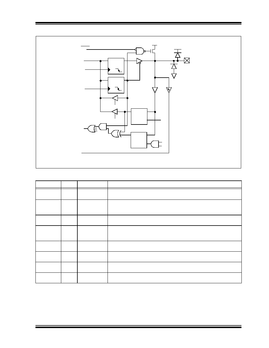
FIGURE 3-7:
BLOCK DIAGRAM OF RB7:RB4 PINS
TABLE 3-3:
PORTB FUNCTIONS
Data Latch
From other
RBPU(1)
P
VDD
I/O
Q
D
CK
Q
D
CK
QD
EN
QD
EN
DATA BUS
WR PORT
WR TRIS
Set RBIF
TRIS Latch
RD TRIS
RD PORT
RB7:RB4 pins
weak
pull-up
RD PORT
Latch
TTL
Buffer
pin
ST
Buffer
RB7:RB6 in Serial Programming mode
Q3
Q1
Note 1: To enable weak pull-ups, set the appropriate TRIS bit(s) and clear the RBPU bit (OPTION_REG<7>).
VSS
VDD
Name
Bit#
Buffer
Function
RB0/INT
bit 0
TTL/ST(1)
Input/output pin or external interrupt input. Internal software
programmable weak pull-up.
RB1/T1OS0/
T1CKI
bit 1
TTL/ST(1)
Input/output pin or Timer1 oscillator output, or Timer1 clock input. Internal
software programmable weak pull-up. See Timer1 section for detailed
operation.
RB2/T1OSI
bit 2
TTL/ST(1)
Input/output pin or Timer1 oscillator input. Internal software programmable
weak pull-up. See Timer1 section for detailed operation.
RB3/CCP1
bit 3
TTL/ST(1)
Input/output pin or Capture 1 input, or Compare 1 output, or PWM1 output.
Internal software programmable weak pull-up. See CCP1 section for
detailed operation.
RB4
bit 4
TTL
Input/output pin (with interrupt-on-change). Internal software programmable
weak pull-up.
RB5
bit 5
TTL
Input/output pin (with interrupt-on-change). Internal software programmable
weak pull-up.
RB6
bit 6
TTL/ST(2)
Input/output pin (with interrupt-on-change). Internal software programmable
weak pull-up. Serial programming clock.
RB7
bit 7
TTL/ST(2)
Input/output pin (with interrupt-on-change). Internal software programmable
weak pull-up. Serial programming data.
Legend: TTL = TTL input, ST = Schmitt Trigger input
Note 1: This buffer is a Schmitt Trigger input when configured as the external interrupt or peripheral input.
2: This buffer is a Schmitt Trigger input when used in Serial Programming mode.
相关PDF资料 |
PDF描述 |
|---|---|
| VI-20Z-IX-B1 | CONVERTER MOD DC/DC 2V 30W |
| PIC16CE623-20I/SO | IC MCU OTP 512X14 EE COMP 18SOIC |
| VI-20Y-IY-B1 | CONVERTER MOD DC/DC 3.3V 33W |
| VI-20Y-IX-B1 | CONVERTER MOD DC/DC 3.3V 49.5W |
| PIC16C712-20I/SS | IC MCU OTP 1KX14 A/D PWM 20SSOP |
相关代理商/技术参数 |
参数描述 |
|---|---|
| PIC16LC716T-04/SO | 功能描述:8位微控制器 -MCU 3.5KB 128 RAM 13 I/O RoHS:否 制造商:Silicon Labs 核心:8051 处理器系列:C8051F39x 数据总线宽度:8 bit 最大时钟频率:50 MHz 程序存储器大小:16 KB 数据 RAM 大小:1 KB 片上 ADC:Yes 工作电源电压:1.8 V to 3.6 V 工作温度范围:- 40 C to + 105 C 封装 / 箱体:QFN-20 安装风格:SMD/SMT |
| PIC16LC716T-04/SS | 功能描述:8位微控制器 -MCU 3.5KB 128 RAM 13 I/O RoHS:否 制造商:Silicon Labs 核心:8051 处理器系列:C8051F39x 数据总线宽度:8 bit 最大时钟频率:50 MHz 程序存储器大小:16 KB 数据 RAM 大小:1 KB 片上 ADC:Yes 工作电源电压:1.8 V to 3.6 V 工作温度范围:- 40 C to + 105 C 封装 / 箱体:QFN-20 安装风格:SMD/SMT |
| PIC16LC716T-04I/SO | 功能描述:8位微控制器 -MCU 3.5KB 128 RAM 13 I/O RoHS:否 制造商:Silicon Labs 核心:8051 处理器系列:C8051F39x 数据总线宽度:8 bit 最大时钟频率:50 MHz 程序存储器大小:16 KB 数据 RAM 大小:1 KB 片上 ADC:Yes 工作电源电压:1.8 V to 3.6 V 工作温度范围:- 40 C to + 105 C 封装 / 箱体:QFN-20 安装风格:SMD/SMT |
| PIC16LC716T-04I/SS | 功能描述:8位微控制器 -MCU 3.5KB 128 RAM 13 I/O RoHS:否 制造商:Silicon Labs 核心:8051 处理器系列:C8051F39x 数据总线宽度:8 bit 最大时钟频率:50 MHz 程序存储器大小:16 KB 数据 RAM 大小:1 KB 片上 ADC:Yes 工作电源电压:1.8 V to 3.6 V 工作温度范围:- 40 C to + 105 C 封装 / 箱体:QFN-20 安装风格:SMD/SMT |
| PIC16LC717/P | 功能描述:8位微控制器 -MCU 3.5KB 256 RAM 16 I/O RoHS:否 制造商:Silicon Labs 核心:8051 处理器系列:C8051F39x 数据总线宽度:8 bit 最大时钟频率:50 MHz 程序存储器大小:16 KB 数据 RAM 大小:1 KB 片上 ADC:Yes 工作电源电压:1.8 V to 3.6 V 工作温度范围:- 40 C to + 105 C 封装 / 箱体:QFN-20 安装风格:SMD/SMT |
发布紧急采购,3分钟左右您将得到回复。