- 您现在的位置:买卖IC网 > PDF目录1964 > PIC16LC72-04I/SP (Microchip Technology)IC MCU OTP 2KX14 A/D PWM 28DIP PDF资料下载
参数资料
| 型号: | PIC16LC72-04I/SP |
| 厂商: | Microchip Technology |
| 文件页数: | 111/111页 |
| 文件大小: | 0K |
| 描述: | IC MCU OTP 2KX14 A/D PWM 28DIP |
| 产品培训模块: | Asynchronous Stimulus 8-bit PIC® Microcontroller Portfolio |
| 标准包装: | 15 |
| 系列: | PIC® 16C |
| 核心处理器: | PIC |
| 芯体尺寸: | 8-位 |
| 速度: | 4MHz |
| 连通性: | I²C,SPI |
| 外围设备: | 欠压检测/复位,POR,PWM,WDT |
| 输入/输出数: | 22 |
| 程序存储器容量: | 3.5KB(2K x 14) |
| 程序存储器类型: | OTP |
| RAM 容量: | 128 x 8 |
| 电压 - 电源 (Vcc/Vdd): | 2.5 V ~ 6 V |
| 数据转换器: | A/D 5x8b |
| 振荡器型: | 外部 |
| 工作温度: | -40°C ~ 85°C |
| 封装/外壳: | 28-DIP(0.300",7.62mm) |
| 包装: | 管件 |
第1页第2页第3页第4页第5页第6页第7页第8页第9页第10页第11页第12页第13页第14页第15页第16页第17页第18页第19页第20页第21页第22页第23页第24页第25页第26页第27页第28页第29页第30页第31页第32页第33页第34页第35页第36页第37页第38页第39页第40页第41页第42页第43页第44页第45页第46页第47页第48页第49页第50页第51页第52页第53页第54页第55页第56页第57页第58页第59页第60页第61页第62页第63页第64页第65页第66页第67页第68页第69页第70页第71页第72页第73页第74页第75页第76页第77页第78页第79页第80页第81页第82页第83页第84页第85页第86页第87页第88页第89页第90页第91页第92页第93页第94页第95页第96页第97页第98页第99页第100页第101页第102页第103页第104页第105页第106页第107页第108页第109页第110页当前第111页
2006 Microchip Technology Inc.
DS39564C-page 97
PIC18FXX2
9.5
PORTE, TRISE and LATE
Registers
This section is only applicable to the PIC18F4X2
devices.
PORTE is a 3-bit wide, bi-directional port. The corre-
sponding Data Direction register is TRISE. Setting a
TRISE bit (= 1) will make the corresponding PORTE pin
an input (i.e., put the corresponding output driver in a
Hi-Impedance mode). Clearing a TRISE bit (= 0) will
make the corresponding PORTE pin an output (i.e., put
the contents of the output latch on the selected pin).
The Data Latch register (LATE) is also memory
mapped. Read-modify-write operations on the LATE
register reads and writes the latched output value for
PORTE.
PORTE has three pins (RE0/RD/AN5, RE1/WR/AN6
and RE2/CS/AN7) which are individually configurable
as inputs or outputs. These pins have Schmitt Trigger
input buffers.
Register 9-1 shows the TRISE register, which also
controls the parallel slave port operation.
PORTE pins are multiplexed with analog inputs. When
selected as an analog input, these pins will read as '0's.
TRISE controls the direction of the RE pins, even when
they are being used as analog inputs. The user must
make sure to keep the pins configured as inputs when
using them as analog inputs.
EXAMPLE 9-5:
INITIALIZING PORTE
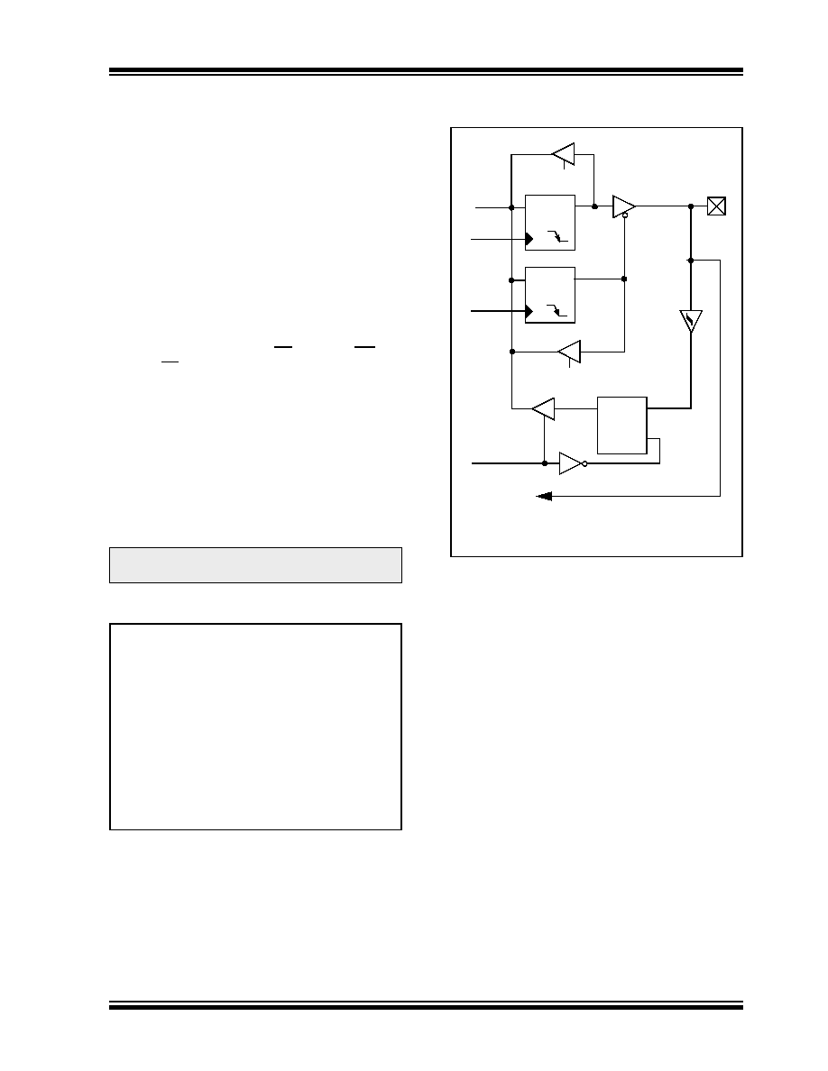
FIGURE 9-9:
PORTE BLOCK DIAGRAM
IN I/O PORT MODE
Note:
On a Power-on Reset, these pins are
configured as analog inputs.
CLRF
PORTE
; Initialize PORTE by
; clearing output
; data latches
CLRF
LATE
; Alternate method
; to clear output
; data latches
MOVLW
0x07
; Configure A/D
MOVWF
ADCON1
; for digital inputs
MOVLW
0x05
; Value used to
; initialize data
; direction
MOVWF
TRISE
; Set RE<0> as inputs
; RE<1> as outputs
; RE<2> as inputs
Data
Bus
WR LATE
WR TRISE
RD PORTE
Data Latch
TRIS Latch
RD TRISE
Schmitt
Trigger
Input
Buffer
Q
D
CK
Q
D
CK
EN
QD
EN
I/O pin(1)
RD LATE
or
PORTE
To Analog Converter
Note 1:
I/O pins have diode protection to VDD and VSS.
相关PDF资料 |
PDF描述 |
|---|---|
| PIC16LC774/L | IC MCU OTP 4KX14 A/D PWM 44PLCC |
| PIC16LC924-04/L | IC MCU OTP 4KX14 LCD DVR 68PLCC |
| PIC16LC926T-I/PT | IC MCU CMOS 20MHZ 8K W/LCD64TQFP |
| PIC16LF1509T-I/SO | IC MCU 8BIT 14KB FLASH 20-SOIC |
| PIC16LF1527-I/MR | MCU PIC 28KB FLASH 64QFN |
相关代理商/技术参数 |
参数描述 |
|---|---|
| PIC16LC72A-04/SO | 功能描述:8位微控制器 -MCU 3.5KB 128 RAM 22 I/O RoHS:否 制造商:Silicon Labs 核心:8051 处理器系列:C8051F39x 数据总线宽度:8 bit 最大时钟频率:50 MHz 程序存储器大小:16 KB 数据 RAM 大小:1 KB 片上 ADC:Yes 工作电源电压:1.8 V to 3.6 V 工作温度范围:- 40 C to + 105 C 封装 / 箱体:QFN-20 安装风格:SMD/SMT |
| PIC16LC72A-04/SP | 功能描述:8位微控制器 -MCU 3.5KB 128 RAM 22 I/O RoHS:否 制造商:Silicon Labs 核心:8051 处理器系列:C8051F39x 数据总线宽度:8 bit 最大时钟频率:50 MHz 程序存储器大小:16 KB 数据 RAM 大小:1 KB 片上 ADC:Yes 工作电源电压:1.8 V to 3.6 V 工作温度范围:- 40 C to + 105 C 封装 / 箱体:QFN-20 安装风格:SMD/SMT |
| PIC16LC72A-04/SS | 功能描述:8位微控制器 -MCU 3.5KB 128 RAM 22 I/O RoHS:否 制造商:Silicon Labs 核心:8051 处理器系列:C8051F39x 数据总线宽度:8 bit 最大时钟频率:50 MHz 程序存储器大小:16 KB 数据 RAM 大小:1 KB 片上 ADC:Yes 工作电源电压:1.8 V to 3.6 V 工作温度范围:- 40 C to + 105 C 封装 / 箱体:QFN-20 安装风格:SMD/SMT |
| PIC16LC72A-04I/ML | 功能描述:8位微控制器 -MCU 3.5KB 128 RAM 22 I/O RoHS:否 制造商:Silicon Labs 核心:8051 处理器系列:C8051F39x 数据总线宽度:8 bit 最大时钟频率:50 MHz 程序存储器大小:16 KB 数据 RAM 大小:1 KB 片上 ADC:Yes 工作电源电压:1.8 V to 3.6 V 工作温度范围:- 40 C to + 105 C 封装 / 箱体:QFN-20 安装风格:SMD/SMT |
| PIC16LC72A-04I/SO | 功能描述:8位微控制器 -MCU 3.5KB 128 RAM 22 I/O RoHS:否 制造商:Silicon Labs 核心:8051 处理器系列:C8051F39x 数据总线宽度:8 bit 最大时钟频率:50 MHz 程序存储器大小:16 KB 数据 RAM 大小:1 KB 片上 ADC:Yes 工作电源电压:1.8 V to 3.6 V 工作温度范围:- 40 C to + 105 C 封装 / 箱体:QFN-20 安装风格:SMD/SMT |
发布紧急采购,3分钟左右您将得到回复。