- 您现在的位置:买卖IC网 > PDF目录11502 > PIC16LC770-I/SO (Microchip Technology)IC MCU OTP 2KX14 A/D PWM 20SOIC PDF资料下载
参数资料
| 型号: | PIC16LC770-I/SO |
| 厂商: | Microchip Technology |
| 文件页数: | 202/220页 |
| 文件大小: | 0K |
| 描述: | IC MCU OTP 2KX14 A/D PWM 20SOIC |
| 产品培训模块: | Asynchronous Stimulus |
| 标准包装: | 38 |
| 系列: | PIC® 16C |
| 核心处理器: | PIC |
| 芯体尺寸: | 8-位 |
| 速度: | 20MHz |
| 连通性: | I²C,SPI |
| 外围设备: | 欠压检测/复位,POR,PWM,WDT |
| 输入/输出数: | 15 |
| 程序存储器容量: | 3.5KB(2K x 14) |
| 程序存储器类型: | OTP |
| RAM 容量: | 256 x 8 |
| 电压 - 电源 (Vcc/Vdd): | 2.5 V ~ 5.5 V |
| 数据转换器: | A/D 6x12b |
| 振荡器型: | 内部 |
| 工作温度: | -40°C ~ 85°C |
| 封装/外壳: | 20-SOIC(0.295",7.50mm 宽) |
| 包装: | 管件 |
| 其它名称: | PIC16LC770I/SO |
第1页第2页第3页第4页第5页第6页第7页第8页第9页第10页第11页第12页第13页第14页第15页第16页第17页第18页第19页第20页第21页第22页第23页第24页第25页第26页第27页第28页第29页第30页第31页第32页第33页第34页第35页第36页第37页第38页第39页第40页第41页第42页第43页第44页第45页第46页第47页第48页第49页第50页第51页第52页第53页第54页第55页第56页第57页第58页第59页第60页第61页第62页第63页第64页第65页第66页第67页第68页第69页第70页第71页第72页第73页第74页第75页第76页第77页第78页第79页第80页第81页第82页第83页第84页第85页第86页第87页第88页第89页第90页第91页第92页第93页第94页第95页第96页第97页第98页第99页第100页第101页第102页第103页第104页第105页第106页第107页第108页第109页第110页第111页第112页第113页第114页第115页第116页第117页第118页第119页第120页第121页第122页第123页第124页第125页第126页第127页第128页第129页第130页第131页第132页第133页第134页第135页第136页第137页第138页第139页第140页第141页第142页第143页第144页第145页第146页第147页第148页第149页第150页第151页第152页第153页第154页第155页第156页第157页第158页第159页第160页第161页第162页第163页第164页第165页第166页第167页第168页第169页第170页第171页第172页第173页第174页第175页第176页第177页第178页第179页第180页第181页第182页第183页第184页第185页第186页第187页第188页第189页第190页第191页第192页第193页第194页第195页第196页第197页第198页第199页第200页第201页当前第202页第203页第204页第205页第206页第207页第208页第209页第210页第211页第212页第213页第214页第215页第216页第217页第218页第219页第220页
PIC16C717/770/771
DS41120B-page 80
Advance Information
2002 Microchip Technology Inc.
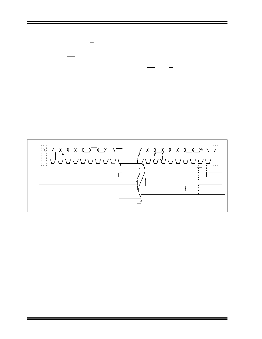
9.2.2.4
SLAVE TRANSMISSION
When the R/W bit of the incoming address byte is set
and an address match occurs, the R/W bit of the SSP-
STAT register is set. The received address is loaded
into the SSPBUF register on the falling edge of the
eighth SCL pulse. The ACK pulse will be sent on the
ninth bit, and the SCL pin is held low. The slave module
automatically stretches the clock by holding the SCL
line low so that the master will be unable to assert
another clock pulse until the slave is finished preparing
the transmit data. The transmit data must be loaded
into the SSPBUF register, which also loads the SSPSR
register. The CKP bit (SSPCON<4>) must then be set
to release the SCL pin from the forced low condition.
The eight data bits are shifted out on the falling edges
of the SCL input. This ensures that the SDA signal is
valid during the SCL high time (Figure 9-10).
The ACK or NACK signal from the master-receiver is
latched on the rising edge of the ninth SCL input pulse.
The master-receiver terminates slave transmission by
sending a NACK. If the SDA line is high (NACK), then
the data transfer is complete. When the NACK is
latched by the slave, the slave logic is RESET which
also resets the R/W bit to ’0’. The slave module then
monitors for another occurrence of the START bit. The
slave firmware knows not to load another byte into the
SSPBUF register by sensing that the buffer is empty
(BF = 0) and the R/W bit has gone low. If the SDA line
is low (ACK), the R/W bit remains high indicating that
the next transmit data must be loaded into the SSPBUF
register.
An MSSP interrupt (SSPIF flag) is generated for each
data transfer byte on the falling edge of the ninth clock
pulse. The SSPIF flag bit must be cleared in software.
The SSPSTAT register is used to determine the status
of the byte transfer.
For more information about the I2C Slave mode, refer
to Application Note AN734, “Using the PICmicro SSP
for Slave I2C Communication”.
FIGURE 9-10:
I2C SLAVE MODE WAVEFORMS FOR TRANSMISSION (7-BIT ADDRESS)
SDA
SCL
SSPIF
BF (SSPSTAT<0>)
CKP (SSPCON<4>)
A7
A6
A5
A4
A3
A2
A1
ACK
D7
D6
D5
D4
D3
D2
D1
D0
NACK
Transmitting Data
R/W = 1
Receiving Address
1
2
3
4
567
89
1
2
3
4
5
6
7
8
9
P
cleared in software
SSPBUF is written in software
From SSP interrupt
service routine
Set bit after writing to SSPBUF
S
Data in
sampled
SCL held low
until SSPBUF
is written
(the SSPBUF must be written-to
before the CKP bit can be set)
R/W
← 0
Master terminates transmission
by responding with NACK
相关PDF资料 |
PDF描述 |
|---|---|
| PIC16C710-20I/SO | IC MCU OTP 512X14 A/D 18SOIC |
| VE-B0B-IY-B1 | CONVERTER MOD DC/DC 95V 50W |
| VE-B04-IY-B1 | CONVERTER MOD DC/DC 48V 50W |
| PIC16C710-20/SS | IC MCU OTP 512X14 A/D 20SSOP |
| PIC24FJ32GA004T-I/ML | IC PIC MCU FLASH 32KB 44QFN |
相关代理商/技术参数 |
参数描述 |
|---|---|
| PIC16LC770T/SO | 功能描述:8位微控制器 -MCU 3.5KB 256 RAM 16 I/O RoHS:否 制造商:Silicon Labs 核心:8051 处理器系列:C8051F39x 数据总线宽度:8 bit 最大时钟频率:50 MHz 程序存储器大小:16 KB 数据 RAM 大小:1 KB 片上 ADC:Yes 工作电源电压:1.8 V to 3.6 V 工作温度范围:- 40 C to + 105 C 封装 / 箱体:QFN-20 安装风格:SMD/SMT |
| PIC16LC770T/SS | 功能描述:8位微控制器 -MCU 3.5KB 256 RAM 16 I/O RoHS:否 制造商:Silicon Labs 核心:8051 处理器系列:C8051F39x 数据总线宽度:8 bit 最大时钟频率:50 MHz 程序存储器大小:16 KB 数据 RAM 大小:1 KB 片上 ADC:Yes 工作电源电压:1.8 V to 3.6 V 工作温度范围:- 40 C to + 105 C 封装 / 箱体:QFN-20 安装风格:SMD/SMT |
| PIC16LC770T-E/SO | 功能描述:8位微控制器 -MCU 3.5KB 256 RAM 16 I/O RoHS:否 制造商:Silicon Labs 核心:8051 处理器系列:C8051F39x 数据总线宽度:8 bit 最大时钟频率:50 MHz 程序存储器大小:16 KB 数据 RAM 大小:1 KB 片上 ADC:Yes 工作电源电压:1.8 V to 3.6 V 工作温度范围:- 40 C to + 105 C 封装 / 箱体:QFN-20 安装风格:SMD/SMT |
| PIC16LC770T-E/SS | 功能描述:8位微控制器 -MCU 3.5KB 256 RAM 16 I/O RoHS:否 制造商:Silicon Labs 核心:8051 处理器系列:C8051F39x 数据总线宽度:8 bit 最大时钟频率:50 MHz 程序存储器大小:16 KB 数据 RAM 大小:1 KB 片上 ADC:Yes 工作电源电压:1.8 V to 3.6 V 工作温度范围:- 40 C to + 105 C 封装 / 箱体:QFN-20 安装风格:SMD/SMT |
| PIC16LC770T-I/SO | 功能描述:8位微控制器 -MCU 3.5KB 256 RAM 16 I/O RoHS:否 制造商:Silicon Labs 核心:8051 处理器系列:C8051F39x 数据总线宽度:8 bit 最大时钟频率:50 MHz 程序存储器大小:16 KB 数据 RAM 大小:1 KB 片上 ADC:Yes 工作电源电压:1.8 V to 3.6 V 工作温度范围:- 40 C to + 105 C 封装 / 箱体:QFN-20 安装风格:SMD/SMT |
发布紧急采购,3分钟左右您将得到回复。