- 您现在的位置:买卖IC网 > PDF目录5244 > LT6202HS5#TRMPBF (Linear Technology)IC OP AMP RRIO 100MHZ TSOT23-5 PDF资料下载
参数资料
| 型号: | LT6202HS5#TRMPBF |
| 厂商: | Linear Technology |
| 文件页数: | 10/28页 |
| 文件大小: | 0K |
| 描述: | IC OP AMP RRIO 100MHZ TSOT23-5 |
| 标准包装: | 500 |
| 放大器类型: | 通用 |
| 电路数: | 1 |
| 输出类型: | 满摆幅 |
| 转换速率: | 25 V/µs |
| 增益带宽积: | 100MHz |
| 电流 - 输入偏压: | 3.8µA |
| 电压 - 输入偏移: | 2600µV |
| 电流 - 电源: | 2.8mA |
| 电流 - 输出 / 通道: | 40mA |
| 电压 - 电源,单路/双路(±): | 2.5 V ~ 12.6 V,±1.25 V ~ 6.3 V |
| 工作温度: | -40°C ~ 125°C |
| 安装类型: | 表面贴装 |
| 封装/外壳: | SOT-23-5 细型,TSOT-23-5 |
| 供应商设备封装: | TSOT-23-5 |
| 包装: | 带卷 (TR) |
| 配用: | DC1813A-E-ND - BOARD SAR ADC LTC2369-18 DC1813A-A-ND - BOARD SAR ADC LTC2370-16 |
第1页第2页第3页第4页第5页第6页第7页第8页第9页当前第10页第11页第12页第13页第14页第15页第16页第17页第18页第19页第20页第21页第22页第23页第24页第25页第26页第27页第28页
LT6202/LT6203/LT6204
18
620234fd
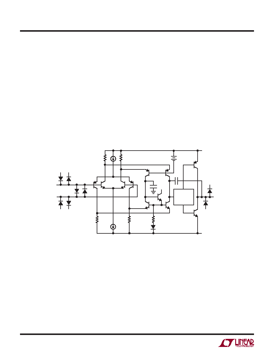
Amplifier Characteristics
Figure 1 shows a simplified schematic of the LT6202/
LT6203/LT6204, which has two input differential ampli-
fiers in parallel that are biased on simultaneously when
the common mode voltage is at least 1.5V from either
rail. This topology allows the input stage to swing from
the positive supply voltage to the negative supply voltage.
As the common mode voltage swings beyond VCC – 1.5V,
current source I1 saturates and current in Q1/Q4 is zero.
Feedback is maintained through the Q2/Q3 differential
amplifier, but with an input gm reduction of 1/2. A similar
effect occurs with I2 when the common mode voltage
swings within 1.5V of the negative rail. The effect of the
gm reduction is a shift in the VOS as I1 or I2 saturate.
APPLICATIONS INFORMATION
Input bias current normally flows out of the + and – inputs.
The magnitude of this current increases when the input
common mode voltage is within 1.5V of the negative rail,
and only Q1/Q4 are active. The polarity of this current
reverses when the input common mode voltage is within
1.5V of the positive rail and only Q2/Q3 are active.
The second stage is a folded cascode and current mir-
ror that converts the input stage differential signals to a
single ended output. Capacitor C1 reduces the unity cross
frequency and improves the frequency stability with-
out degrading the gain bandwidth of the amplifier. The
differential drive generator supplies current to the output
transistors that swing from rail-to-rail.
DIFFERENTIAL
DRIVE
GENERATOR
+
–
R1
R2
R3
R4
R5
Q2
Q3
Q5
Q6
Q9
Q8
Q7
Q10
Q11
Q1
Q4
I1
I2
D3
D2
D1
DESD2
DESD4
DESD3
DESD1
DESD5
DESD6
+
–
VBIAS
CM
C1
+V
–V
V+
V–
6203/04 F01
Figure 1. Simplified Schematic
相关PDF资料 |
PDF描述 |
|---|---|
| MCP6231RT-E/OT | IC OPAMP 1.8V SNGL R-R SOT23-5 |
| AS168X-CB1DG320 | CIRCUIT BRKR THERMAL 32.0A 1POLE |
| TA45-A344H200C0 | CIRCUIT BRKR THERMAL 20A 2POLE |
| TA45-A443HJ10C0 | CIRCUIT BRKR THERMAL 1A 2POLE |
| TA45-A341F100C0 | CIRCUIT BRKR THERMAL 10A 2POLE |
相关代理商/技术参数 |
参数描述 |
|---|---|
| PIC16LC774T/L | 功能描述:8位微控制器 -MCU 7KB 256 RAM 33 I/O RoHS:否 制造商:Silicon Labs 核心:8051 处理器系列:C8051F39x 数据总线宽度:8 bit 最大时钟频率:50 MHz 程序存储器大小:16 KB 数据 RAM 大小:1 KB 片上 ADC:Yes 工作电源电压:1.8 V to 3.6 V 工作温度范围:- 40 C to + 105 C 封装 / 箱体:QFN-20 安装风格:SMD/SMT |
| PIC16LC774T/PQ | 功能描述:8位微控制器 -MCU 7KB 256 RAM 33 I/O RoHS:否 制造商:Silicon Labs 核心:8051 处理器系列:C8051F39x 数据总线宽度:8 bit 最大时钟频率:50 MHz 程序存储器大小:16 KB 数据 RAM 大小:1 KB 片上 ADC:Yes 工作电源电压:1.8 V to 3.6 V 工作温度范围:- 40 C to + 105 C 封装 / 箱体:QFN-20 安装风格:SMD/SMT |
| PIC16LC774T/PT | 功能描述:8位微控制器 -MCU 7KB 256 RAM 33 I/O RoHS:否 制造商:Silicon Labs 核心:8051 处理器系列:C8051F39x 数据总线宽度:8 bit 最大时钟频率:50 MHz 程序存储器大小:16 KB 数据 RAM 大小:1 KB 片上 ADC:Yes 工作电源电压:1.8 V to 3.6 V 工作温度范围:- 40 C to + 105 C 封装 / 箱体:QFN-20 安装风格:SMD/SMT |
| PIC16LC774T-I/L | 功能描述:8位微控制器 -MCU 7KB 256 RAM 33 I/O RoHS:否 制造商:Silicon Labs 核心:8051 处理器系列:C8051F39x 数据总线宽度:8 bit 最大时钟频率:50 MHz 程序存储器大小:16 KB 数据 RAM 大小:1 KB 片上 ADC:Yes 工作电源电压:1.8 V to 3.6 V 工作温度范围:- 40 C to + 105 C 封装 / 箱体:QFN-20 安装风格:SMD/SMT |
| PIC16LC774T-I/PQ | 功能描述:8位微控制器 -MCU 7KB 256 RAM 33 I/O RoHS:否 制造商:Silicon Labs 核心:8051 处理器系列:C8051F39x 数据总线宽度:8 bit 最大时钟频率:50 MHz 程序存储器大小:16 KB 数据 RAM 大小:1 KB 片上 ADC:Yes 工作电源电压:1.8 V to 3.6 V 工作温度范围:- 40 C to + 105 C 封装 / 箱体:QFN-20 安装风格:SMD/SMT |
发布紧急采购,3分钟左右您将得到回复。