- 您现在的位置:买卖IC网 > PDF目录11779 > PIC16LF720-I/SS (Microchip Technology)MCU PIC 2K FLASH 20-SSOP PDF资料下载
参数资料
| 型号: | PIC16LF720-I/SS |
| 厂商: | Microchip Technology |
| 文件页数: | 53/135页 |
| 文件大小: | 0K |
| 描述: | MCU PIC 2K FLASH 20-SSOP |
| 产品培训模块: | 8-bit PIC® Microcontroller Portfolio |
| 标准包装: | 67 |
| 系列: | PIC® XLP™ 16F |
| 核心处理器: | PIC |
| 芯体尺寸: | 8-位 |
| 速度: | 16MHz |
| 连通性: | I²C,SPI,UART/USART |
| 外围设备: | 欠压检测/复位,POR,PWM,WDT |
| 输入/输出数: | 17 |
| 程序存储器容量: | 3.5KB(2K x 14) |
| 程序存储器类型: | 闪存 |
| RAM 容量: | 128 x 8 |
| 电压 - 电源 (Vcc/Vdd): | 1.8 V ~ 3.6 V |
| 数据转换器: | A/D 12x8b |
| 振荡器型: | 内部 |
| 工作温度: | -40°C ~ 85°C |
| 封装/外壳: | 28-SSOP(0.209",5.30mm 宽) |
| 包装: | 管件 |
第1页第2页第3页第4页第5页第6页第7页第8页第9页第10页第11页第12页第13页第14页第15页第16页第17页第18页第19页第20页第21页第22页第23页第24页第25页第26页第27页第28页第29页第30页第31页第32页第33页第34页第35页第36页第37页第38页第39页第40页第41页第42页第43页第44页第45页第46页第47页第48页第49页第50页第51页第52页当前第53页第54页第55页第56页第57页第58页第59页第60页第61页第62页第63页第64页第65页第66页第67页第68页第69页第70页第71页第72页第73页第74页第75页第76页第77页第78页第79页第80页第81页第82页第83页第84页第85页第86页第87页第88页第89页第90页第91页第92页第93页第94页第95页第96页第97页第98页第99页第100页第101页第102页第103页第104页第105页第106页第107页第108页第109页第110页第111页第112页第113页第114页第115页第116页第117页第118页第119页第120页第121页第122页第123页第124页第125页第126页第127页第128页第129页第130页第131页第132页第133页第134页第135页
PIC16(L)F720/721
DS41430C-page 24
Preliminary
2010-2011 Microchip Technology Inc.
2.3
PCL and PCLATH
The Program Counter (PC) is 13 bits wide. The low
byte comes from the PCL register, which is a readable
and writable register. The high byte (PC<12:8>) is not
directly readable or writable and comes from
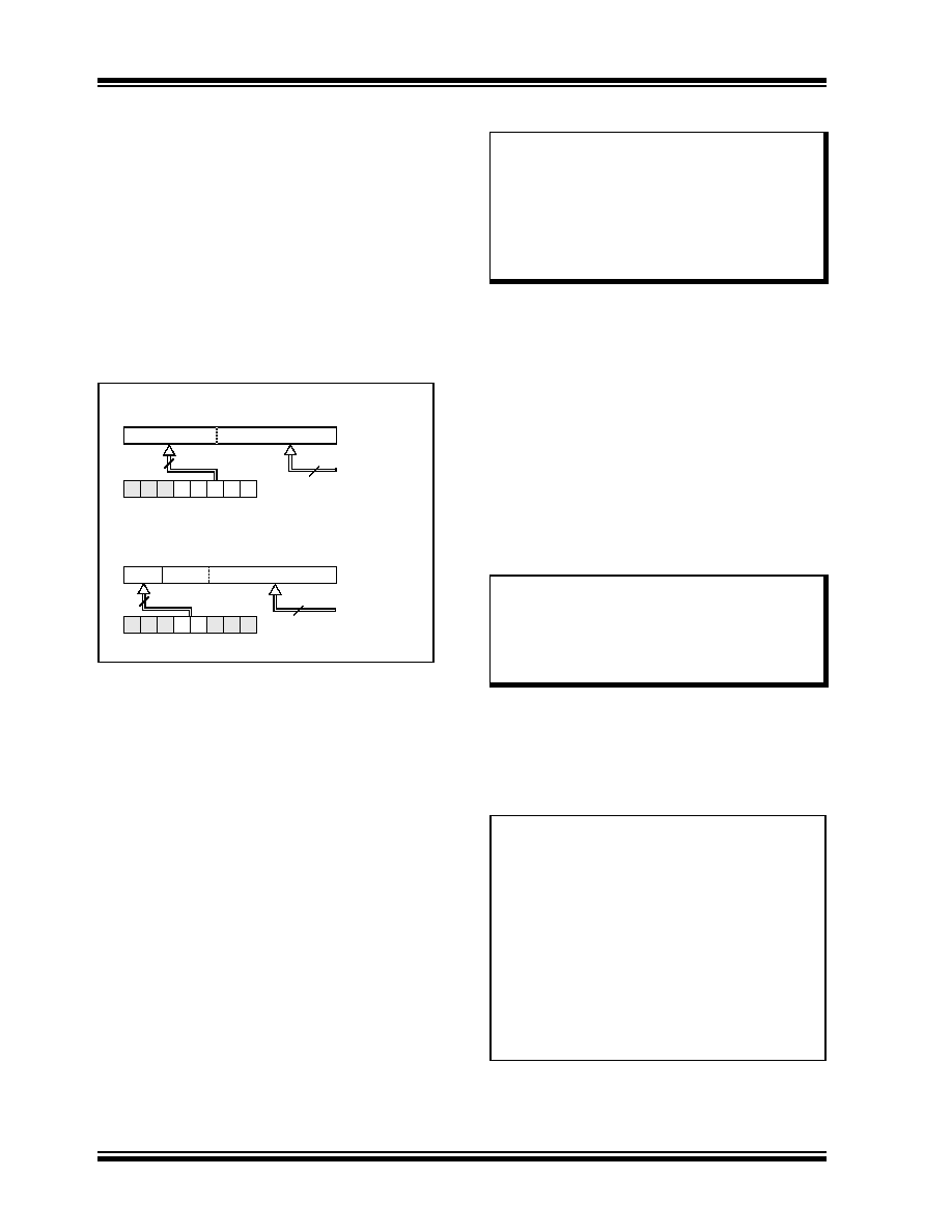
PCLATH. On any Reset, the PC is cleared. Figure 2-5
shows the two situations for the loading of the PC. The
upper example in Figure 2-5 shows how the PC is
loaded on a write to PCL (PCLATH<4:0>
PCH).
The lower example in Figure 2-5 shows how the PC is
loaded
during
a
CALL
or
GOTO
instruction
(PCLATH<4:3>
PCH).
FIGURE 2-5:
LOADING OF PC IN
DIFFERENT SITUATIONS
2.3.1
COMPUTED GOTO
A computed GOTO is accomplished by adding an offset
to the program counter (ADDWF PCL). When perform-
ing a table read using a computed GOTO method, care
should be exercised if the table location crosses a PCL
memory boundary (each 256-byte block). Refer to the
Application Note AN556, “Implementing a Table Read”
(DS00556).
2.3.2
STACK
All devices have an 8-level x 13-bit wide hardware
not part of either program or data space and the Stack
Pointer is not readable or writable. The PC is PUSHed
onto the stack when a CALL instruction is executed or
an interrupt causes a branch. The stack is POPed in
the event of a RETURN, RETLW or a RETFIE instruction
execution. PCLATH is not affected by a PUSH or POP
operation.
The stack operates as a circular buffer. This means that
after the stack has been PUSHed eight times, the ninth
PUSH overwrites the value that was stored from the
first PUSH. The tenth PUSH overwrites the second
PUSH (and so on).
2.4
Program Memory Paging
All devices are capable of addressing a continuous 8K
word block of program memory. The CALL and GOTO
instructions provide only 11 bits of address to allow
branching within any 2K program memory page. When
doing a CALL or GOTO instruction, the upper 2 bits of
the address are provided by PCLATH<4:3>. When
doing a CALL or GOTO instruction, the user must ensure
that the page select bits are programmed so that the
desired program memory page is addressed. If a return
from a CALL instruction (or interrupt) is executed, the
entire 13-bit PC is POPed off the stack. Therefore,
manipulation of the PCLATH<4:3> bits is not required
for the RETURN instructions (which POPs the address
from the stack).
Example 2-1 shows the calling of a subroutine in
page 1 of the program memory. This example assumes
that PCLATH is saved and restored by the Interrupt
Service Routine (if interrupts are used).
EXAMPLE 2-1:
CALL OF A SUBROUTINE
IN PAGE 1 FROM PAGE 0
PC
12
8 7
0
5
PCLATH<4:0>
PCLATH
Instruction with
ALU Result
GOTO, CALL
Opcode<10:0>
8
PC
12 11 10
0
11
PCLATH<4:3>
PCH
PCL
87
2
PCLATH
PCH
PCL
PCL as
Destination
Note 1: There are no Status bits to indicate stack
overflow or stack underflow conditions.
2: There are no instructions/mnemonics
called PUSH or POP. These are actions
that occur from the execution of the
CALL, RETURN, RETLW and RETFIE
instructions or the vectoring to an
interrupt address.
Note:
The contents of the PCLATH register are
unchanged after a RETURN or RETFIE
instruction is executed. The user must
rewrite the contents of the PCLATH regis-
ter for any subsequent subroutine calls or
GOTO instructions.
ORG 500h
PAGESEL SUB_P1 ;Select page 1
;(800h-FFFh)
CALL
SUB1_P1 ;Call subroutine in
:
;page 1 (800h-FFFh)
:
ORG
900h
;page 1 (800h-FFFh)
SUB1_P1
:
;called subroutine
;page 1 (800h-FFFh)
:
RETURN
;return to
;Call subroutine
;in page 0
;(000h-7FFh)
相关PDF资料 |
PDF描述 |
|---|---|
| PIC16F720-I/SS | MCU PIC 2K FLASH 20-SSOP |
| PIC16F526-E/P | IC PIC MCU FLASH 1KX12 14DIP |
| PIC16F610-I/P | IC PIC MCU FLASH 1KX14 14DIP |
| VE-B4N-IX-F3 | CONVERTER MOD DC/DC 18.5V 75W |
| PIC12HV752-I/P | IC MCU 8BIT 1024B FLASH 8-PDIP |
相关代理商/技术参数 |
参数描述 |
|---|---|
| PIC16LF720T-I/ML | 功能描述:8位微控制器 -MCU 3.5 KB FLASH 128 B SRAM, 18 I/O RoHS:否 制造商:Silicon Labs 核心:8051 处理器系列:C8051F39x 数据总线宽度:8 bit 最大时钟频率:50 MHz 程序存储器大小:16 KB 数据 RAM 大小:1 KB 片上 ADC:Yes 工作电源电压:1.8 V to 3.6 V 工作温度范围:- 40 C to + 105 C 封装 / 箱体:QFN-20 安装风格:SMD/SMT |
| PIC16LF720T-I/SO | 功能描述:8位微控制器 -MCU 3.5 KB FLASH 128 B SRAM, 18 I/O RoHS:否 制造商:Silicon Labs 核心:8051 处理器系列:C8051F39x 数据总线宽度:8 bit 最大时钟频率:50 MHz 程序存储器大小:16 KB 数据 RAM 大小:1 KB 片上 ADC:Yes 工作电源电压:1.8 V to 3.6 V 工作温度范围:- 40 C to + 105 C 封装 / 箱体:QFN-20 安装风格:SMD/SMT |
| PIC16LF720T-I/SS | 功能描述:8位微控制器 -MCU 3.5 KB FLASH 128 B SRAM, 18 I/O RoHS:否 制造商:Silicon Labs 核心:8051 处理器系列:C8051F39x 数据总线宽度:8 bit 最大时钟频率:50 MHz 程序存储器大小:16 KB 数据 RAM 大小:1 KB 片上 ADC:Yes 工作电源电压:1.8 V to 3.6 V 工作温度范围:- 40 C to + 105 C 封装 / 箱体:QFN-20 安装风格:SMD/SMT |
| PIC16LF721-E/ML | 功能描述:8位微控制器 -MCU 7 KB FLASH 256 B SRAM, 18 I/O RoHS:否 制造商:Silicon Labs 核心:8051 处理器系列:C8051F39x 数据总线宽度:8 bit 最大时钟频率:50 MHz 程序存储器大小:16 KB 数据 RAM 大小:1 KB 片上 ADC:Yes 工作电源电压:1.8 V to 3.6 V 工作温度范围:- 40 C to + 105 C 封装 / 箱体:QFN-20 安装风格:SMD/SMT |
| PIC16LF721-E/P | 功能描述:8位微控制器 -MCU 7 KB FLASH 256 B SRAM, 18 I/O RoHS:否 制造商:Silicon Labs 核心:8051 处理器系列:C8051F39x 数据总线宽度:8 bit 最大时钟频率:50 MHz 程序存储器大小:16 KB 数据 RAM 大小:1 KB 片上 ADC:Yes 工作电源电压:1.8 V to 3.6 V 工作温度范围:- 40 C to + 105 C 封装 / 箱体:QFN-20 安装风格:SMD/SMT |
发布紧急采购,3分钟左右您将得到回复。