- 您现在的位置:买卖IC网 > PDF目录11406 > PIC16LF737T-I/SS (Microchip Technology)IC PIC MCU FLASH 4KX14 28SSOP PDF资料下载
参数资料
| 型号: | PIC16LF737T-I/SS |
| 厂商: | Microchip Technology |
| 文件页数: | 215/231页 |
| 文件大小: | 0K |
| 描述: | IC PIC MCU FLASH 4KX14 28SSOP |
| 产品培训模块: | Asynchronous Stimulus |
| 标准包装: | 2,100 |
| 系列: | PIC® 16F |
| 核心处理器: | PIC |
| 芯体尺寸: | 8-位 |
| 速度: | 10MHz |
| 连通性: | I²C,SPI,UART/USART |
| 外围设备: | 欠压检测/复位,POR,PWM,WDT |
| 输入/输出数: | 25 |
| 程序存储器容量: | 7KB(4K x 14) |
| 程序存储器类型: | 闪存 |
| RAM 容量: | 368 x 8 |
| 电压 - 电源 (Vcc/Vdd): | 2 V ~ 5.5 V |
| 数据转换器: | A/D 11x10b |
| 振荡器型: | 内部 |
| 工作温度: | -40°C ~ 85°C |
| 封装/外壳: | 28-SSOP(0.209",5.30mm 宽) |
| 包装: | 带卷 (TR) |
第1页第2页第3页第4页第5页第6页第7页第8页第9页第10页第11页第12页第13页第14页第15页第16页第17页第18页第19页第20页第21页第22页第23页第24页第25页第26页第27页第28页第29页第30页第31页第32页第33页第34页第35页第36页第37页第38页第39页第40页第41页第42页第43页第44页第45页第46页第47页第48页第49页第50页第51页第52页第53页第54页第55页第56页第57页第58页第59页第60页第61页第62页第63页第64页第65页第66页第67页第68页第69页第70页第71页第72页第73页第74页第75页第76页第77页第78页第79页第80页第81页第82页第83页第84页第85页第86页第87页第88页第89页第90页第91页第92页第93页第94页第95页第96页第97页第98页第99页第100页第101页第102页第103页第104页第105页第106页第107页第108页第109页第110页第111页第112页第113页第114页第115页第116页第117页第118页第119页第120页第121页第122页第123页第124页第125页第126页第127页第128页第129页第130页第131页第132页第133页第134页第135页第136页第137页第138页第139页第140页第141页第142页第143页第144页第145页第146页第147页第148页第149页第150页第151页第152页第153页第154页第155页第156页第157页第158页第159页第160页第161页第162页第163页第164页第165页第166页第167页第168页第169页第170页第171页第172页第173页第174页第175页第176页第177页第178页第179页第180页第181页第182页第183页第184页第185页第186页第187页第188页第189页第190页第191页第192页第193页第194页第195页第196页第197页第198页第199页第200页第201页第202页第203页第204页第205页第206页第207页第208页第209页第210页第211页第212页第213页第214页当前第215页第216页第217页第218页第219页第220页第221页第222页第223页第224页第225页第226页第227页第228页第229页第230页第231页
2004 Microchip Technology Inc.
DS30498C-page 45
PIC16F7X7
4.7.3.2
Returning to Primary Oscillator with
a Reset
A Reset will clear SCS<1:0> back to ‘00’. The
sequence for starting the primary oscillator following a
Reset is the same for all forms of Reset, including
POR. There is no transition sequence from the
alternate system clock to the primary system clock on
a Reset condition. Instead, the device will reset the
state of the OSCCON register and default to the
primary system clock. The sequence of events that
take place after this will depend upon the value of the
FOSC bits in the Configuration register. If the external
oscillator is configured as a crystal (HS, XT or LP), the
CPU will be held in the Q1 state until 1024 clock cycles
have transpired on the primary
clock. This is
necessary because the crystal oscillator had been
powered down until the time of the transition.
During
the
oscillator
start-up
time,
instruction
execution and/or peripheral operation is suspended.
If the primary system clock is either RC, EC or INTRC,
the CPU will begin operating on the first Q1 cycle
following the wake-up event. This means that there is
no oscillator start-up time required because the
primary clock is already stable; however, there is a
delay between the wake-up event and the following
Q2. An internal delay timer of 5-10
s will suspend
operation after the Reset to allow the CPU to become
ready for code execution. The CPU and peripheral
clock will be held in the first Q1.
The sequence of events is as follows:
1.
A device Reset is asserted from one of many
sources (WDT, BOR, MCLR, etc.).
2.
The device resets and the CPU start-up timer is
enabled if in Sleep mode. The device is held in
Reset until the CPU start-up time-out is
complete.
3.
If the primary system clock is configured as an
external oscillator (HS, XT, LP), then the OST
will be active waiting for 1024 clocks of the pri-
mary system clock. While waiting for the OST,
the device will be held in Reset. The OST and
CPU start-up timers run in parallel.
4.
After both the CPU start-up timer and the
Oscillator Start-up Timer have timed out, the
device will wait for one additional clock cycle
and instruction execution will begin.
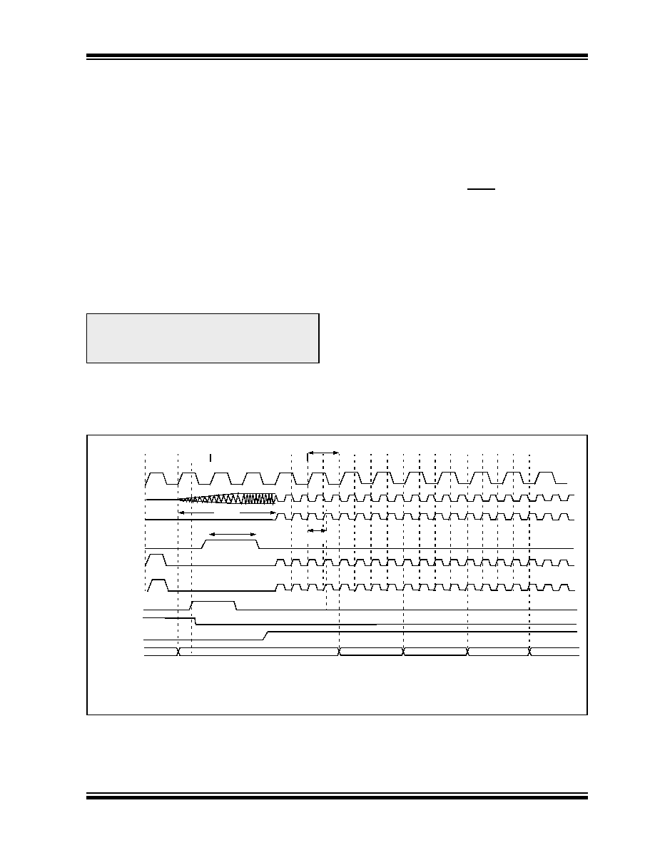
FIGURE 4-10:
TIMING LP CLOCK TO PRIMARY SYSTEM CLOCK AFTER RESET (HS, XT, LP)
Note:
If Two-Speed Clock Start-up mode is
enabled, the INTRC will act as the system
clock until the Oscillator Start-up Timer has
timed out.
Q4
Q1
Q3 Q4
Q1 Q2
OSC1
Peripheral
Sleep
Program
PC
0000h
T1OSI
TOST(4)
Q3
TT1P(1)
Q4
OSC2
OSTS
System Clock
0001h
Q1 Q2 Q3 Q4 Q1 Q2
Clock
Counter
0004h
0005h
0003h
Q1 Q2 Q3 Q4
Reset
TEPU(3)
Note 1:
TT1P = 30.52
s.
2:
TOSC = 50 ns minimum.
3:
TEPU = 5-10
s.
4:
Refer to parameter D032 in Section 18.0 “Electrical Characteristics”.
CPU Start-up
TOSC(2)
相关PDF资料 |
PDF描述 |
|---|---|
| VE-26N-CV-F2 | CONVERTER MOD DC/DC 18.5V 150W |
| VE-26L-CV-F4 | CONVERTER MOD DC/DC 28V 150W |
| GRM2196S2A4R2CD01D | CAP CER 4.2PF 100V S2H 0805 |
| GRM2196S2A3R8CD01D | CAP CER 3.8PF 100V S2H 0805 |
| GRM2196S2A3R4CD01D | CAP CER 3.4PF 100V S2H 0805 |
相关代理商/技术参数 |
参数描述 |
|---|---|
| PIC16LF73-I/ML | 功能描述:8位微控制器 -MCU 7KB 192 RAM 22 I/O RoHS:否 制造商:Silicon Labs 核心:8051 处理器系列:C8051F39x 数据总线宽度:8 bit 最大时钟频率:50 MHz 程序存储器大小:16 KB 数据 RAM 大小:1 KB 片上 ADC:Yes 工作电源电压:1.8 V to 3.6 V 工作温度范围:- 40 C to + 105 C 封装 / 箱体:QFN-20 安装风格:SMD/SMT |
| PIC16LF73-I/SO | 功能描述:8位微控制器 -MCU 7KB 192 RAM 22 I/O RoHS:否 制造商:Silicon Labs 核心:8051 处理器系列:C8051F39x 数据总线宽度:8 bit 最大时钟频率:50 MHz 程序存储器大小:16 KB 数据 RAM 大小:1 KB 片上 ADC:Yes 工作电源电压:1.8 V to 3.6 V 工作温度范围:- 40 C to + 105 C 封装 / 箱体:QFN-20 安装风格:SMD/SMT |
| PIC16LF73-I/SO | 制造商:Microchip Technology Inc 功能描述:8BIT FLASH MCU SMD 16LF73 SOIC28 |
| PIC16LF73-I/SOG | 功能描述:8位微控制器 -MCU 7KB 192 RAM 22 I/O Lead Free Package RoHS:否 制造商:Silicon Labs 核心:8051 处理器系列:C8051F39x 数据总线宽度:8 bit 最大时钟频率:50 MHz 程序存储器大小:16 KB 数据 RAM 大小:1 KB 片上 ADC:Yes 工作电源电压:1.8 V to 3.6 V 工作温度范围:- 40 C to + 105 C 封装 / 箱体:QFN-20 安装风格:SMD/SMT |
| PIC16LF73-I/SP | 功能描述:8位微控制器 -MCU 7KB 192 RAM 22 I/O RoHS:否 制造商:Silicon Labs 核心:8051 处理器系列:C8051F39x 数据总线宽度:8 bit 最大时钟频率:50 MHz 程序存储器大小:16 KB 数据 RAM 大小:1 KB 片上 ADC:Yes 工作电源电压:1.8 V to 3.6 V 工作温度范围:- 40 C to + 105 C 封装 / 箱体:QFN-20 安装风格:SMD/SMT |
发布紧急采购,3分钟左右您将得到回复。