- 您现在的位置:买卖IC网 > PDF目录3837 > PIC16LF84A-04/SS (Microchip Technology)IC MCU FLASH 1KX14 EE 20SSOP PDF资料下载
参数资料
| 型号: | PIC16LF84A-04/SS |
| 厂商: | Microchip Technology |
| 文件页数: | 10/80页 |
| 文件大小: | 0K |
| 描述: | IC MCU FLASH 1KX14 EE 20SSOP |
| 产品培训模块: | Asynchronous Stimulus 8-bit PIC® Microcontroller Portfolio |
| 标准包装: | 67 |
| 系列: | PIC® 16F |
| 核心处理器: | PIC |
| 芯体尺寸: | 8-位 |
| 速度: | 4MHz |
| 外围设备: | POR,WDT |
| 输入/输出数: | 13 |
| 程序存储器容量: | 1.75KB(1K x 14) |
| 程序存储器类型: | 闪存 |
| EEPROM 大小: | 64 x 8 |
| RAM 容量: | 68 x 8 |
| 电压 - 电源 (Vcc/Vdd): | 2 V ~ 5.5 V |
| 振荡器型: | 外部 |
| 工作温度: | 0°C ~ 70°C |
| 封装/外壳: | 20-SSOP(0.209",5.30mm 宽) |
| 包装: | 管件 |
| 产品目录页面: | 638 (CN2011-ZH PDF) |
第1页第2页第3页第4页第5页第6页第7页第8页第9页当前第10页第11页第12页第13页第14页第15页第16页第17页第18页第19页第20页第21页第22页第23页第24页第25页第26页第27页第28页第29页第30页第31页第32页第33页第34页第35页第36页第37页第38页第39页第40页第41页第42页第43页第44页第45页第46页第47页第48页第49页第50页第51页第52页第53页第54页第55页第56页第57页第58页第59页第60页第61页第62页第63页第64页第65页第66页第67页第68页第69页第70页第71页第72页第73页第74页第75页第76页第77页第78页第79页第80页
PIC16F8X
DS30430C-page 18
1998 Microchip Technology Inc.
4.3
Program Counter: PCL and PCLATH
The Program Counter (PC) is 13-bits wide. The low
byte is the PCL register, which is a readable and
writable register. The high byte of the PC (PC<12:8>) is
not directly readable nor writable and comes from the
PCLATH register. The PCLATH (PC latch high) register
is a holding register for PC<12:8>. The contents of
PCLATH are transferred to the upper byte of the
program counter when the PC is loaded with a new
value. This occurs during a CALL, GOTO or a write to
PCL. The high bits of PC are loaded from PCLATH as
shown in Figure 4-1.
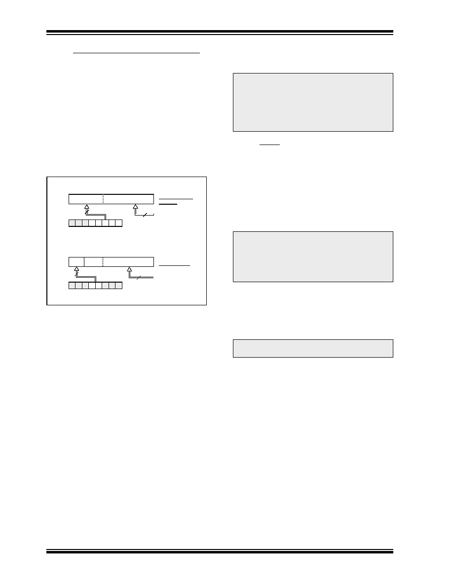
FIGURE 4-1:
LOADING OF PC IN
DIFFERENT SITUATIONS
4.3.1
COMPUTED GOTO
A computed GOTO is accomplished by adding an offset
to the program counter (ADDWF PCL). When doing a
table read using a computed GOTO method, care should
be exercised if the table location crosses a PCL memory
boundary (each 256 word block). Refer to the application
note
“Implementing a Table Read” (AN556).
4.3.2
PROGRAM MEMORY PAGING
The PIC16F83 and PIC16CR83 have 512 words of pro-
gram memory. The PIC16F84 and PIC16CR84 have
1K of program memory. The CALL and GOTO instruc-
tions have an 11-bit address range. This 11-bit address
range allows a branch within a 2K program memory
page size. For future PIC16F8X program memory
expansion, there must be another two bits to specify
the program memory page. These paging bits come
from the PCLATH<4:3> bits (Figure 4-1). When doing a
CALL
or a GOTO instruction, the user must ensure that
these page bits (PCLATH<4:3>) are programmed to
the desired program memory page. If a CALL instruc-
tion (or interrupt) is executed, the entire 13-bit PC is
“pushed” onto the stack (see next section). Therefore,
manipulation of the PCLATH<4:3> is not required for
the return instructions (which “pops” the PC from the
stack).
4.4
Stack
The PIC16FXX has an 8 deep x 13-bit wide hardware
stack (Figure 4-1). The stack space is not part of either
program or data space and the stack pointer is not
readable or writable.
The entire 13-bit PC is “pushed” onto the stack when a
CALL
instruction is executed or an interrupt is acknowl-
edged. The stack is “popped” in the event of a
RETURN,
RETLW
or a RETFIE instruction execution.
PCLATH is not affected by a push or a pop operation.
The stack operates as a circular buffer. That is, after the
stack has been pushed eight times, the ninth push over-
writes the value that was stored from the first push. The
tenth push overwrites the second push (and so on).
If the stack is effectively popped nine times, the PC
value is the same as the value from the first pop.
PC
12
8 7
0
5
PCLATH<4:0>
PCLATH
INST with PCL
as dest
ALU result
GOTO, CALL
Opcode <10:0>
8
PC
12 11 10
0
11
PCLATH<4:3>
PCH
PCL
87
2
PCLATH
PCH
PCL
Note:
The PIC16F8X ignores the PCLATH<4:3>
bits, which are used for program memory
pages 1, 2 and 3 (0800h - 1FFFh). The
use of PCLATH<4:3> as general purpose
R/W bits is not recommended since this
may affect upward compatibility with
future products.
Note:
There are no instruction mnemonics
called push or pop. These are actions that
occur from the execution of the CALL,
RETURN,
RETLW,
and RETFIE instruc-
tions, or the vectoring to an interrupt
address.
Note:
There are no status bits to indicate stack
overflow or stack underflow conditions.
相关PDF资料 |
PDF描述 |
|---|---|
| PIC18LF6527T-I/PT | IC PIC MCU FLASH 24KX16 64TQFP |
| 008016020000601 | CONN RACK & PANEL MALE 20P |
| 008016038000601 | CONN RACK & PANEL MALE 38P |
| DSPIC33FJ16GS502-I/SP | IC DSPIC MCU/DSP 16K 28-DIP |
| 516-038-000-161 | CONN PLUG 38POS RACK AND PANEL |
相关代理商/技术参数 |
参数描述 |
|---|---|
| PIC16LF84AT-04/SO | 功能描述:8位微控制器 -MCU 1.75KB 68 RAM 13 I/O RoHS:否 制造商:Silicon Labs 核心:8051 处理器系列:C8051F39x 数据总线宽度:8 bit 最大时钟频率:50 MHz 程序存储器大小:16 KB 数据 RAM 大小:1 KB 片上 ADC:Yes 工作电源电压:1.8 V to 3.6 V 工作温度范围:- 40 C to + 105 C 封装 / 箱体:QFN-20 安装风格:SMD/SMT |
| PIC16LF84AT-04/SS | 功能描述:8位微控制器 -MCU 1.75KB 68 RAM 13 I/O RoHS:否 制造商:Silicon Labs 核心:8051 处理器系列:C8051F39x 数据总线宽度:8 bit 最大时钟频率:50 MHz 程序存储器大小:16 KB 数据 RAM 大小:1 KB 片上 ADC:Yes 工作电源电压:1.8 V to 3.6 V 工作温度范围:- 40 C to + 105 C 封装 / 箱体:QFN-20 安装风格:SMD/SMT |
| PIC16LF84AT-04I/SO | 功能描述:8位微控制器 -MCU 1.75KB 68 RAM 13 I/O RoHS:否 制造商:Silicon Labs 核心:8051 处理器系列:C8051F39x 数据总线宽度:8 bit 最大时钟频率:50 MHz 程序存储器大小:16 KB 数据 RAM 大小:1 KB 片上 ADC:Yes 工作电源电压:1.8 V to 3.6 V 工作温度范围:- 40 C to + 105 C 封装 / 箱体:QFN-20 安装风格:SMD/SMT |
| PIC16LF84AT-04I/SS | 功能描述:8位微控制器 -MCU 1.75KB 68 RAM 13 I/O RoHS:否 制造商:Silicon Labs 核心:8051 处理器系列:C8051F39x 数据总线宽度:8 bit 最大时钟频率:50 MHz 程序存储器大小:16 KB 数据 RAM 大小:1 KB 片上 ADC:Yes 工作电源电压:1.8 V to 3.6 V 工作温度范围:- 40 C to + 105 C 封装 / 箱体:QFN-20 安装风格:SMD/SMT |
| PIC16LF84T-04/SO | 功能描述:8位微控制器 -MCU 1.75KB 68 RAM 13 I/O RoHS:否 制造商:Silicon Labs 核心:8051 处理器系列:C8051F39x 数据总线宽度:8 bit 最大时钟频率:50 MHz 程序存储器大小:16 KB 数据 RAM 大小:1 KB 片上 ADC:Yes 工作电源电压:1.8 V to 3.6 V 工作温度范围:- 40 C to + 105 C 封装 / 箱体:QFN-20 安装风格:SMD/SMT |
发布紧急采购,3分钟左右您将得到回复。