- 您现在的位置:买卖IC网 > PDF目录1964 > PIC16LF872-I/SS (Microchip Technology)IC MCU FLASH 2KX14 EE A/D 28SSOP PDF资料下载
参数资料
| 型号: | PIC16LF872-I/SS |
| 厂商: | Microchip Technology |
| 文件页数: | 5/167页 |
| 文件大小: | 0K |
| 描述: | IC MCU FLASH 2KX14 EE A/D 28SSOP |
| 产品培训模块: | Asynchronous Stimulus 8-bit PIC® Microcontroller Portfolio |
| 标准包装: | 47 |
| 系列: | PIC® 16F |
| 核心处理器: | PIC |
| 芯体尺寸: | 8-位 |
| 速度: | 20MHz |
| 连通性: | I²C,SPI |
| 外围设备: | 欠压检测/复位,POR,PWM,WDT |
| 输入/输出数: | 22 |
| 程序存储器容量: | 3.5KB(2K x 14) |
| 程序存储器类型: | 闪存 |
| EEPROM 大小: | 64 x 8 |
| RAM 容量: | 128 x 8 |
| 电压 - 电源 (Vcc/Vdd): | 2.2 V ~ 5.5 V |
| 数据转换器: | A/D 5x10b |
| 振荡器型: | 外部 |
| 工作温度: | -40°C ~ 85°C |
| 封装/外壳: | 28-SSOP(0.209",5.30mm 宽) |
| 包装: | 管件 |
| 产品目录页面: | 639 (CN2011-ZH PDF) |
第1页第2页第3页第4页当前第5页第6页第7页第8页第9页第10页第11页第12页第13页第14页第15页第16页第17页第18页第19页第20页第21页第22页第23页第24页第25页第26页第27页第28页第29页第30页第31页第32页第33页第34页第35页第36页第37页第38页第39页第40页第41页第42页第43页第44页第45页第46页第47页第48页第49页第50页第51页第52页第53页第54页第55页第56页第57页第58页第59页第60页第61页第62页第63页第64页第65页第66页第67页第68页第69页第70页第71页第72页第73页第74页第75页第76页第77页第78页第79页第80页第81页第82页第83页第84页第85页第86页第87页第88页第89页第90页第91页第92页第93页第94页第95页第96页第97页第98页第99页第100页第101页第102页第103页第104页第105页第106页第107页第108页第109页第110页第111页第112页第113页第114页第115页第116页第117页第118页第119页第120页第121页第122页第123页第124页第125页第126页第127页第128页第129页第130页第131页第132页第133页第134页第135页第136页第137页第138页第139页第140页第141页第142页第143页第144页第145页第146页第147页第148页第149页第150页第151页第152页第153页第154页第155页第156页第157页第158页第159页第160页第161页第162页第163页第164页第165页第166页第167页
102
8048C–AVR–02/12
ATtiny43U
14. USI – Universal Serial Interface
14.1
Features
Two-wire Synchronous Data Transfer (Master or Slave)
Three-wire Synchronous Data Transfer (Master or Slave)
Data Received Interrupt
Wakeup from Idle Mode
In Two-wire Mode: Wake-up from All Sleep Modes, Including Power-down Mode
Two-wire Start Condition Detector with Interrupt Capability
14.2
Overview
The Universal Serial Interface (USI), provides the basic hardware resources needed for serial
communication. Combined with a minimum of control software, the USI allows significantly
higher transfer rates and uses less code space than solutions based on software only. Interrupts
are included to minimize the processor load.
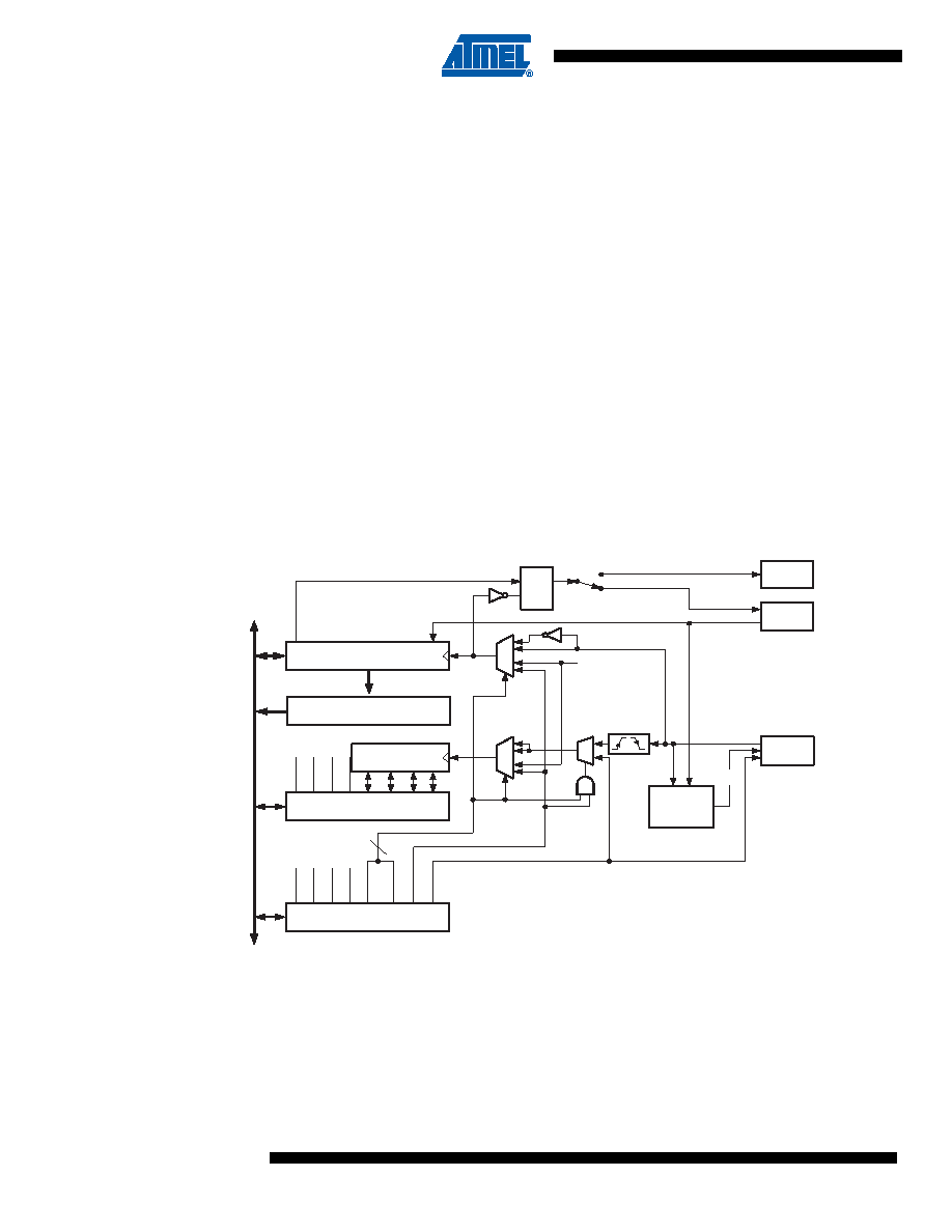
A simplified block diagram of the USI is shown in Figure 14-1 on page 102. For actual placement
of I/O pins, refer to “Pinout of ATtiny43U” on page 2. CPU accessible I/O Registers, including I/O
bits and I/O pins, are shown in bold. The device-specific I/O Register and bit locations are listed
Figure 14-1. Universal Serial Interface, Block Diagram
The 8-bit USI Data Register (USIDR) contains the incoming and outgoing data. It is directly
accessible via the data bus but a copy of the contents is also placed in the USI Buffer Register
(USIBR) where it can be retrieved later. If reading the USI Data Register directly, the register
must be read as quickly as possible to ensure that no data is lost.
The most significant bit of the USI Data Register is connected to one of two output pins (depend-
ing on the mode configuration, see Table 14-1 on page 110). There is a transparent latch
between the output of the USI Data Register and the output pin, which delays the change of data
DATA
BUS
USIPF
USITC
USICLK
USICS0
USICS1
USIOIF
USIOIE
USIDC
USISIF
USIWM0
USIWM1
USISIE
Bit7
Two-wire Clock
Control Unit
DO
(Output only)
DI/SDA
(Input/Open Drain)
USCK/SCL
(Input/Open Drain)
4-bit Counter
USIDR
USISR
DQ
LE
USICR
CLOCK
HOLD
TIM0 COMP
Bit0
[1]
3
0
1
2
3
0
1
2
0
1
2
USIDB
相关PDF资料 |
PDF描述 |
|---|---|
| PIC16LF877A-I/ML | IC MCU FLASH 8KX14 A/D 44QFN |
| PIC16LF88-I/ML | IC MCU FLASH 4KX14 EEPROM 28QFN |
| PIC17C44-33/L | IC MCU OTP 8KX16 PWM 44PLCC |
| PIC17C766-33I/L | IC MCU OTP 16KX16 A/D 84PLCC |
| PIC18C452-I/L | IC MCU OTP 16KX16 A/D 44PLCC |
相关代理商/技术参数 |
参数描述 |
|---|---|
| PIC16LF872T-I/SO | 功能描述:8位微控制器 -MCU 3.5KB 128 RAM 22 I/O RoHS:否 制造商:Silicon Labs 核心:8051 处理器系列:C8051F39x 数据总线宽度:8 bit 最大时钟频率:50 MHz 程序存储器大小:16 KB 数据 RAM 大小:1 KB 片上 ADC:Yes 工作电源电压:1.8 V to 3.6 V 工作温度范围:- 40 C to + 105 C 封装 / 箱体:QFN-20 安装风格:SMD/SMT |
| PIC16LF872T-I/SS | 功能描述:8位微控制器 -MCU 3.5KB 128 RAM 22 I/O RoHS:否 制造商:Silicon Labs 核心:8051 处理器系列:C8051F39x 数据总线宽度:8 bit 最大时钟频率:50 MHz 程序存储器大小:16 KB 数据 RAM 大小:1 KB 片上 ADC:Yes 工作电源电压:1.8 V to 3.6 V 工作温度范围:- 40 C to + 105 C 封装 / 箱体:QFN-20 安装风格:SMD/SMT |
| PIC16LF873-04/SO | 功能描述:8位微控制器 -MCU 7KB 192 RAM 22 I/O RoHS:否 制造商:Silicon Labs 核心:8051 处理器系列:C8051F39x 数据总线宽度:8 bit 最大时钟频率:50 MHz 程序存储器大小:16 KB 数据 RAM 大小:1 KB 片上 ADC:Yes 工作电源电压:1.8 V to 3.6 V 工作温度范围:- 40 C to + 105 C 封装 / 箱体:QFN-20 安装风格:SMD/SMT |
| PIC16LF873-04/SP | 功能描述:8位微控制器 -MCU 7KB 192 RAM 22 I/O RoHS:否 制造商:Silicon Labs 核心:8051 处理器系列:C8051F39x 数据总线宽度:8 bit 最大时钟频率:50 MHz 程序存储器大小:16 KB 数据 RAM 大小:1 KB 片上 ADC:Yes 工作电源电压:1.8 V to 3.6 V 工作温度范围:- 40 C to + 105 C 封装 / 箱体:QFN-20 安装风格:SMD/SMT |
| PIC16LF873-04I/SO | 功能描述:8位微控制器 -MCU 7KB 192 RAM 22 I/O RoHS:否 制造商:Silicon Labs 核心:8051 处理器系列:C8051F39x 数据总线宽度:8 bit 最大时钟频率:50 MHz 程序存储器大小:16 KB 数据 RAM 大小:1 KB 片上 ADC:Yes 工作电源电压:1.8 V to 3.6 V 工作温度范围:- 40 C to + 105 C 封装 / 箱体:QFN-20 安装风格:SMD/SMT |
发布紧急采购,3分钟左右您将得到回复。