- 您现在的位置:买卖IC网 > PDF目录10853 > PIC16LV54AT-02/SO (Microchip Technology)IC MCU OTP 512X12 18SOIC PDF资料下载
参数资料
| 型号: | PIC16LV54AT-02/SO |
| 厂商: | Microchip Technology |
| 文件页数: | 89/194页 |
| 文件大小: | 0K |
| 描述: | IC MCU OTP 512X12 18SOIC |
| 标准包装: | 1,100 |
| 系列: | PIC® 16C |
| 核心处理器: | PIC |
| 芯体尺寸: | 8-位 |
| 速度: | 2MHz |
| 外围设备: | POR,WDT |
| 输入/输出数: | 12 |
| 程序存储器容量: | 768B(512 x 12) |
| 程序存储器类型: | OTP |
| RAM 容量: | 25 x 8 |
| 电压 - 电源 (Vcc/Vdd): | 2 V ~ 3.8 V |
| 振荡器型: | 外部 |
| 工作温度: | 0°C ~ 70°C |
| 封装/外壳: | 18-SOIC(0.295",7.50mm 宽) |
| 包装: | 带卷 (TR) |
第1页第2页第3页第4页第5页第6页第7页第8页第9页第10页第11页第12页第13页第14页第15页第16页第17页第18页第19页第20页第21页第22页第23页第24页第25页第26页第27页第28页第29页第30页第31页第32页第33页第34页第35页第36页第37页第38页第39页第40页第41页第42页第43页第44页第45页第46页第47页第48页第49页第50页第51页第52页第53页第54页第55页第56页第57页第58页第59页第60页第61页第62页第63页第64页第65页第66页第67页第68页第69页第70页第71页第72页第73页第74页第75页第76页第77页第78页第79页第80页第81页第82页第83页第84页第85页第86页第87页第88页当前第89页第90页第91页第92页第93页第94页第95页第96页第97页第98页第99页第100页第101页第102页第103页第104页第105页第106页第107页第108页第109页第110页第111页第112页第113页第114页第115页第116页第117页第118页第119页第120页第121页第122页第123页第124页第125页第126页第127页第128页第129页第130页第131页第132页第133页第134页第135页第136页第137页第138页第139页第140页第141页第142页第143页第144页第145页第146页第147页第148页第149页第150页第151页第152页第153页第154页第155页第156页第157页第158页第159页第160页第161页第162页第163页第164页第165页第166页第167页第168页第169页第170页第171页第172页第173页第174页第175页第176页第177页第178页第179页第180页第181页第182页第183页第184页第185页第186页第187页第188页第189页第190页第191页第192页第193页第194页
PIC18F2450/4450
2006 Microchip Technology Inc.
Advance Information
DS39760A-page 177
The value in the ADRESH:ADRESL registers is not
modified for a Power-on Reset. The ADRESH:ADRESL
registers will contain unknown data after a Power-on
Reset.
After the A/D module has been configured as desired, the
selected channel must be acquired before the conver-
sion is started. The analog input channels must have
their corresponding TRIS bits selected as an input. To
determine acquisition time, see Section 16.1 “A/D
Acquisition Requirements”. After this acquisition time
has elapsed, the A/D conversion can be started. An
acquisition time can be programmed to occur between
setting the GO/DONE bit and the actual start of the
conversion.
The following steps should be followed to perform an
A/D conversion:
1.
Configure the A/D module:
Configure analog pins, voltage reference and
digital I/O (ADCON1)
Select A/D input channel (ADCON0)
Select A/D acquisition time (ADCON2)
Select A/D conversion clock (ADCON2)
Turn on A/D module (ADCON0)
2.
Configure A/D interrupt (if desired):
Clear ADIF bit
Set ADIE bit
Set GIE bit
3.
Wait the required acquisition time (if required).
4.
Start conversion:
Set GO/DONE bit (ADCON0 register)
5.
Wait for A/D conversion to complete, by either:
Polling for the GO/DONE bit to be cleared
OR
Waiting for the A/D interrupt
6.
Read A/D Result registers (ADRESH:ADRESL);
clear bit ADIF, if required.
7.
For next conversion, go to step 1 or step 2, as
required. The A/D conversion time per bit is
defined as TAD. A minimum wait of 3 TAD is
required before the next acquisition starts.
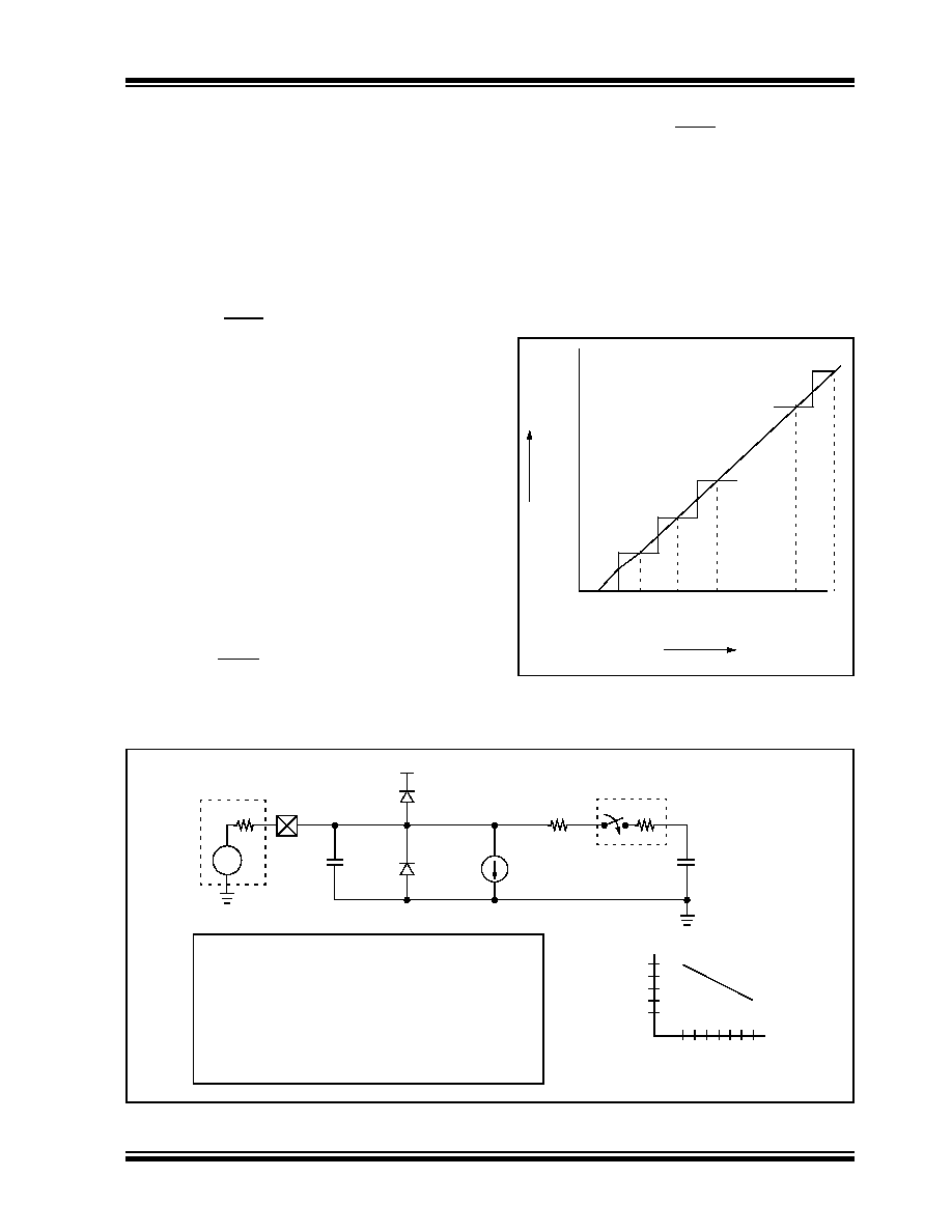
FIGURE 16-2:
A/D TRANSFER FUNCTION
FIGURE 16-3:
ANALOG INPUT MODEL
Dig
it
a
lCo
d
e
Ou
tp
u
t
3FEh
003h
002h
001h
000h
0.
5
LS
B
1
L
S
B
1.
5
LS
B
2
L
S
B
2.
5
LS
B
102
2
L
S
B
10
22
.5
L
S
B
3
L
S
B
Analog Input Voltage
3FFh
102
3
L
S
B
10
23
.5
L
S
B
VAIN
CPIN
Rs
ANx
5 pF
VT = 0.6V
ILEAKAGE
RIC
≤ 1k
Sampling
Switch
SS
RSS
CHOLD = 25 pF
VSS
VDD
±100 nA
Legend: CPIN
VT
ILEAKAGE
RIC
SS
CHOLD
= Input Capacitance
= Threshold Voltage
= Leakage Current at the pin due to
= Interconnect Resistance
= Sampling Switch
= Sample/hold Capacitance (from DAC)
various junctions
= Sampling Switch Resistance
RSS
VDD
6V
Sampling Switch
5V
4V
3V
2V
12
3
4
(k
Ω)
相关PDF资料 |
PDF描述 |
|---|---|
| PIC16LF877T-04/PT | IC MCU FLASH 8KX14 EE A/D 44TQFP |
| PIC16LF877T-04/PQ | IC MCU FLASH 8KX14 EE A/D 44MQFP |
| PIC16LF871T-I/PT | IC MCU FLASH 2KX14 EE A/D 44TQFP |
| PIC16LF871T-I/L | IC MCU FLASH 2KX14 EE A/D 44PLCC |
| PIC16LF877T-04/L | IC MCU FLASH 8KX14 EE A/D 44PLCC |
相关代理商/技术参数 |
参数描述 |
|---|---|
| PIC16LV923-04I/PT | 制造商:Microchip Technology Inc 功能描述: |
| PIC17C02-ME | 制造商:Microchip Technology Inc 功能描述:ELECTRONIC COMPONENT |
| PIC17C42/JW | 制造商:Microchip Technology Inc 功能描述: |
| PIC17C42-25/L | 制造商:Microchip Technology 功能描述:MCU 8-bit PIC17 PIC RISC 4KB EPROM 5V 44-Pin PLCC Tube |
| PIC17C4225L | 制造商:MICROCHIP 功能描述:New |
发布紧急采购,3分钟左右您将得到回复。