- 您现在的位置:买卖IC网 > PDF目录10852 > PIC17C42AT-33E/PT (Microchip Technology)IC MCU OTP 2KX16 PWM 44TQFP PDF资料下载
参数资料
| 型号: | PIC17C42AT-33E/PT |
| 厂商: | Microchip Technology |
| 文件页数: | 219/241页 |
| 文件大小: | 0K |
| 描述: | IC MCU OTP 2KX16 PWM 44TQFP |
| 标准包装: | 1,200 |
| 系列: | PIC® 17C |
| 核心处理器: | PIC |
| 芯体尺寸: | 8-位 |
| 速度: | 33MHz |
| 连通性: | UART/USART |
| 外围设备: | POR,PWM,WDT |
| 输入/输出数: | 33 |
| 程序存储器容量: | 4KB(2K x 16) |
| 程序存储器类型: | OTP |
| RAM 容量: | 232 x 8 |
| 电压 - 电源 (Vcc/Vdd): | 4.5 V ~ 6 V |
| 振荡器型: | 外部 |
| 工作温度: | -40°C ~ 125°C |
| 封装/外壳: | 44-TQFP |
| 包装: | 带卷 (TR) |
| 配用: | AC164315-ND - MODULE SKT MPLAB PM3 44TQFP |
第1页第2页第3页第4页第5页第6页第7页第8页第9页第10页第11页第12页第13页第14页第15页第16页第17页第18页第19页第20页第21页第22页第23页第24页第25页第26页第27页第28页第29页第30页第31页第32页第33页第34页第35页第36页第37页第38页第39页第40页第41页第42页第43页第44页第45页第46页第47页第48页第49页第50页第51页第52页第53页第54页第55页第56页第57页第58页第59页第60页第61页第62页第63页第64页第65页第66页第67页第68页第69页第70页第71页第72页第73页第74页第75页第76页第77页第78页第79页第80页第81页第82页第83页第84页第85页第86页第87页第88页第89页第90页第91页第92页第93页第94页第95页第96页第97页第98页第99页第100页第101页第102页第103页第104页第105页第106页第107页第108页第109页第110页第111页第112页第113页第114页第115页第116页第117页第118页第119页第120页第121页第122页第123页第124页第125页第126页第127页第128页第129页第130页第131页第132页第133页第134页第135页第136页第137页第138页第139页第140页第141页第142页第143页第144页第145页第146页第147页第148页第149页第150页第151页第152页第153页第154页第155页第156页第157页第158页第159页第160页第161页第162页第163页第164页第165页第166页第167页第168页第169页第170页第171页第172页第173页第174页第175页第176页第177页第178页第179页第180页第181页第182页第183页第184页第185页第186页第187页第188页第189页第190页第191页第192页第193页第194页第195页第196页第197页第198页第199页第200页第201页第202页第203页第204页第205页第206页第207页第208页第209页第210页第211页第212页第213页第214页第215页第216页第217页第218页当前第219页第220页第221页第222页第223页第224页第225页第226页第227页第228页第229页第230页第231页第232页第233页第234页第235页第236页第237页第238页第239页第240页第241页
1996 Microchip Technology Inc.
DS30412C-page 79
PIC17C4X
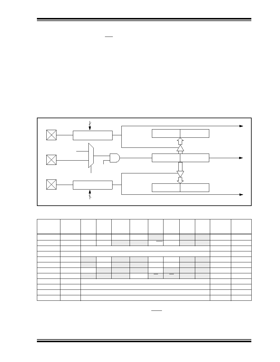
12.2.2
DUAL CAPTURE REGISTER MODE
This mode is selected by setting CA1/PR3. A block dia-
gram is shown in Figure 12-8. In this mode, TMR3 runs
without a period register and increments from 0000h to
FFFFh and rolls over to 0000h. The TMR3 interrupt
Flag (TMR3IF) is set on this roll over. The TMR3IF bit
must be cleared in software.
Registers PR3H/CA1H and PR3L/CA1L make a 16-bit
capture register (Capture1). It captures events on pin
RB0/CAP1. Capture mode is congured by the
CA1ED1 and CA1ED0 bits. Capture1 Interrupt Flag bit
(CA1IF) is set on the capture event. The corresponding
interrupt mask bit is CA1IE. The Capture1 Overow
Status bit is CA1OVF.
The Capture2 overow status ag bit is double buff-
ered. The master bit is set if one captured word is
already residing in the Capture2 register and another
“event” has occurred on the RB1/CA2 pin. The new
event will not transfer the TMR3 value to the capture
register which protects the previous unread capture
value. When the user reads both the high and the low
bytes (in any order) of the Capture2 register, the master
overow bit is transferred to the slave overow bit
(CA2OVF) and then the master bit is reset. The user
can then read TCON2 to determine the value of
CA2OVF.
The operation of the Capture1 feature is identical to
Capture2 (as described in Section 12.2.1).
FIGURE 12-8: TIMER3 WITH TWO CAPTURE REGISTERS BLOCK DIAGRAM
TABLE 12-5:
REGISTERS ASSOCIATED WITH CAPTURE
Address
Name
Bit 7
Bit 6
Bit 5
Bit 4
Bit 3
Bit 2
Bit 1
Bit 0
Value on
Power-on
Reset
Value on all
other resets
(Note1)
16h, Bank 3
TCON1
CA2ED1
CA2ED0
CA1ED1
CA1ED0
T16
TMR3CS TMR2CS TMR1CS 0000 0000
0000 0000
17h, Bank 3
TCON2
CA2OVF CA1OVF
PWM2ON
PWM1ON CA1/PR3 TMR3ON TMR2ON TMR1ON 0000 0000
0000 0000
12h, Bank 2
TMR3L
TMR3 register; low byte
xxxx xxxx
uuuu uuuu
13h, Bank 2
TMR3H
TMR3 register; high byte
xxxx xxxx
uuuu uuuu
16h, Bank 1
PIR
RBIF
TMR3IF
TMR2IF
TMR1IF
CA2IF
CA1IF
TXIF
RCIF
0000 0010
17h, Bank 1
PIE
RBIE
TMR3IE
TMR2IE
TMR1IE
CA2IE
CA1IE
TXIE
RCIE
0000 0000
07h, Unbanked INTSTA
PEIF
T0CKIF
T0IF
INTF
PEIE
T0CKIE
T0IE
INTE
0000 0000
06h, Unbanked CPUSTA
—
STKAV
GLINTD
TO
PD
—
--11 11--
--11 qq--
16h, Bank 2
PR3L/CA1L
Timer3 period register, low byte/capture1 register, low byte
xxxx xxxx
uuuu uuuu
17h, Bank 2
PR3H/CA1H Timer3 period register, high byte/capture1 register, high byte
xxxx xxxx
uuuu uuuu
14h, Bank 3
CA2L
Capture2 low byte
xxxx xxxx
uuuu uuuu
15h, Bank 3
CA2H
Capture2 high byte
xxxx xxxx
uuuu uuuu
Legend: x = unknown, u = unchanged, - = unimplemented read as '0', q - value depends on condition,
shaded cells are not used by Capture.
Note 1:
Other (non power-up) resets include: external reset through MCLR and WDT Timer Reset.
2
RB0/CAP1
Edge Select
Prescaler Select
PR3H/CA1H
PR3L/CA1L
TMR3H
TMR3L
RB5/TCLK3
0
1
Fosc/4
RB1/CAP2
Edge Select
Prescaler Select
2
CA2ED1, CA2ED0
(TCON1<7:6>)
CA2H
CA2L
Set CA2IF
(PIR<3>)
Set TMR3IF
(PIR<6>)
Set CA1IF
(PIR<2>)
Capture Enable
TMR3ON
(TCON2<2>)
TMR3CS
(TCON1<2>)
CA1ED1, CA1ED0
(TCON1<5:4>)
相关PDF资料 |
PDF描述 |
|---|---|
| PIC17C42AT-33E/PQ | IC MCU OTP 2KX16 PWM 44-MQFP |
| PIC17C42AT-33E/L | IC MCU OTP 2KX16 PWM 44PLCC |
| PIC17C42AT-25/PT | IC MCU OTP 2KX16 PWM 44TQFP |
| PIC17C42AT-25/PQ | IC MCU OTP 2KX16 PWM 44-MQFP |
| PIC17C42AT-25/L | IC MCU OTP 2KX16 PWM 44PLCC |
相关代理商/技术参数 |
参数描述 |
|---|---|
| PIC17C42AT-33I/L | 功能描述:8位微控制器 -MCU 4KB 232 RAM 33 I/O RoHS:否 制造商:Silicon Labs 核心:8051 处理器系列:C8051F39x 数据总线宽度:8 bit 最大时钟频率:50 MHz 程序存储器大小:16 KB 数据 RAM 大小:1 KB 片上 ADC:Yes 工作电源电压:1.8 V to 3.6 V 工作温度范围:- 40 C to + 105 C 封装 / 箱体:QFN-20 安装风格:SMD/SMT |
| PIC17C42AT-33I/PQ | 功能描述:8位微控制器 -MCU 4KB 232 RAM 33 I/O RoHS:否 制造商:Silicon Labs 核心:8051 处理器系列:C8051F39x 数据总线宽度:8 bit 最大时钟频率:50 MHz 程序存储器大小:16 KB 数据 RAM 大小:1 KB 片上 ADC:Yes 工作电源电压:1.8 V to 3.6 V 工作温度范围:- 40 C to + 105 C 封装 / 箱体:QFN-20 安装风格:SMD/SMT |
| PIC17C42AT-33I/PT | 功能描述:8位微控制器 -MCU 4KB 232 RAM 33 I/O RoHS:否 制造商:Silicon Labs 核心:8051 处理器系列:C8051F39x 数据总线宽度:8 bit 最大时钟频率:50 MHz 程序存储器大小:16 KB 数据 RAM 大小:1 KB 片上 ADC:Yes 工作电源电压:1.8 V to 3.6 V 工作温度范围:- 40 C to + 105 C 封装 / 箱体:QFN-20 安装风格:SMD/SMT |
| PIC17C43/JW | 功能描述:8位微控制器 -MCU 64KB 3328 RAM w/ECAN RoHS:否 制造商:Silicon Labs 核心:8051 处理器系列:C8051F39x 数据总线宽度:8 bit 最大时钟频率:50 MHz 程序存储器大小:16 KB 数据 RAM 大小:1 KB 片上 ADC:Yes 工作电源电压:1.8 V to 3.6 V 工作温度范围:- 40 C to + 105 C 封装 / 箱体:QFN-20 安装风格:SMD/SMT |
| PIC17C43-16/L | 功能描述:8位微控制器 -MCU 8KB 454 RAM 33 I/O RoHS:否 制造商:Silicon Labs 核心:8051 处理器系列:C8051F39x 数据总线宽度:8 bit 最大时钟频率:50 MHz 程序存储器大小:16 KB 数据 RAM 大小:1 KB 片上 ADC:Yes 工作电源电压:1.8 V to 3.6 V 工作温度范围:- 40 C to + 105 C 封装 / 箱体:QFN-20 安装风格:SMD/SMT |
发布紧急采购,3分钟左右您将得到回复。