- 您现在的位置:买卖IC网 > PDF目录11248 > PIC17C752-16I/L (Microchip Technology)IC MCU OTP 8KX16 A/D PWM 68PLCC PDF资料下载
参数资料
| 型号: | PIC17C752-16I/L |
| 厂商: | Microchip Technology |
| 文件页数: | 142/159页 |
| 文件大小: | 0K |
| 描述: | IC MCU OTP 8KX16 A/D PWM 68PLCC |
| 产品培训模块: | Asynchronous Stimulus |
| 标准包装: | 19 |
| 系列: | PIC® 17C |
| 核心处理器: | PIC |
| 芯体尺寸: | 8-位 |
| 速度: | 16MHz |
| 连通性: | I²C,SPI,UART/USART |
| 外围设备: | 欠压检测/复位,POR,PWM,WDT |
| 输入/输出数: | 50 |
| 程序存储器容量: | 16KB(8K x 16) |
| 程序存储器类型: | OTP |
| RAM 容量: | 454 x 8 |
| 电压 - 电源 (Vcc/Vdd): | 4.5 V ~ 5.5 V |
| 数据转换器: | A/D 12x10b |
| 振荡器型: | 外部 |
| 工作温度: | -40°C ~ 85°C |
| 封装/外壳: | 68-LCC(J 形引线) |
| 包装: | 管件 |
| 配用: | AC164308-ND - MODULE SKT FOR PM3 68PLCC DVA17XL681-ND - DEVICE ADAPTER FOR PIC17C752 DM173001-ND - KIT DEVELOPMENT PICDEM17 AC174007-ND - MODULE SKT PROMATEII 68PLCC AC164024-ND - ADAPTER PICSTART PLUS 68PLCC |
第1页第2页第3页第4页第5页第6页第7页第8页第9页第10页第11页第12页第13页第14页第15页第16页第17页第18页第19页第20页第21页第22页第23页第24页第25页第26页第27页第28页第29页第30页第31页第32页第33页第34页第35页第36页第37页第38页第39页第40页第41页第42页第43页第44页第45页第46页第47页第48页第49页第50页第51页第52页第53页第54页第55页第56页第57页第58页第59页第60页第61页第62页第63页第64页第65页第66页第67页第68页第69页第70页第71页第72页第73页第74页第75页第76页第77页第78页第79页第80页第81页第82页第83页第84页第85页第86页第87页第88页第89页第90页第91页第92页第93页第94页第95页第96页第97页第98页第99页第100页第101页第102页第103页第104页第105页第106页第107页第108页第109页第110页第111页第112页第113页第114页第115页第116页第117页第118页第119页第120页第121页第122页第123页第124页第125页第126页第127页第128页第129页第130页第131页第132页第133页第134页第135页第136页第137页第138页第139页第140页第141页当前第142页第143页第144页第145页第146页第147页第148页第149页第150页第151页第152页第153页第154页第155页第156页第157页第158页第159页
PIC17C7XX
DS30289B-page 82
2000 Microchip Technology Inc.
10.5
PORTE and DDRE Register
PORTE is a 4-bit bi-directional port. The corresponding
data direction register is DDRE. A ’1’ in DDRE config-
ures the corresponding port pin as an input. A ’0’ in the
DDRE register configures the corresponding port pin
as an output. Reading PORTE reads the status of the
pins, whereas writing to PORTE will write to the port
latch. PORTE is multiplexed with the system bus.
When operating as the system bus, PORTE contains
the
control
signals
for
the
address/data
bus
(AD15:AD0). These control signals are Address Latch
Enable (ALE), Output Enable (OE) and Write (WR).
The control signals OE and WR are active low signals.
The timing for the system bus is shown in the Electrical
Specifications section.
Example 10-5 shows an instruction sequence to initial-
ize PORTE. The Bank Select Register (BSR) must be
selected to Bank 1 for the port to be initialized. The fol-
lowing example uses the MOVLB instruction to load the
BSR register for bank selection.
EXAMPLE 10-5:
INITIALIZING PORTE
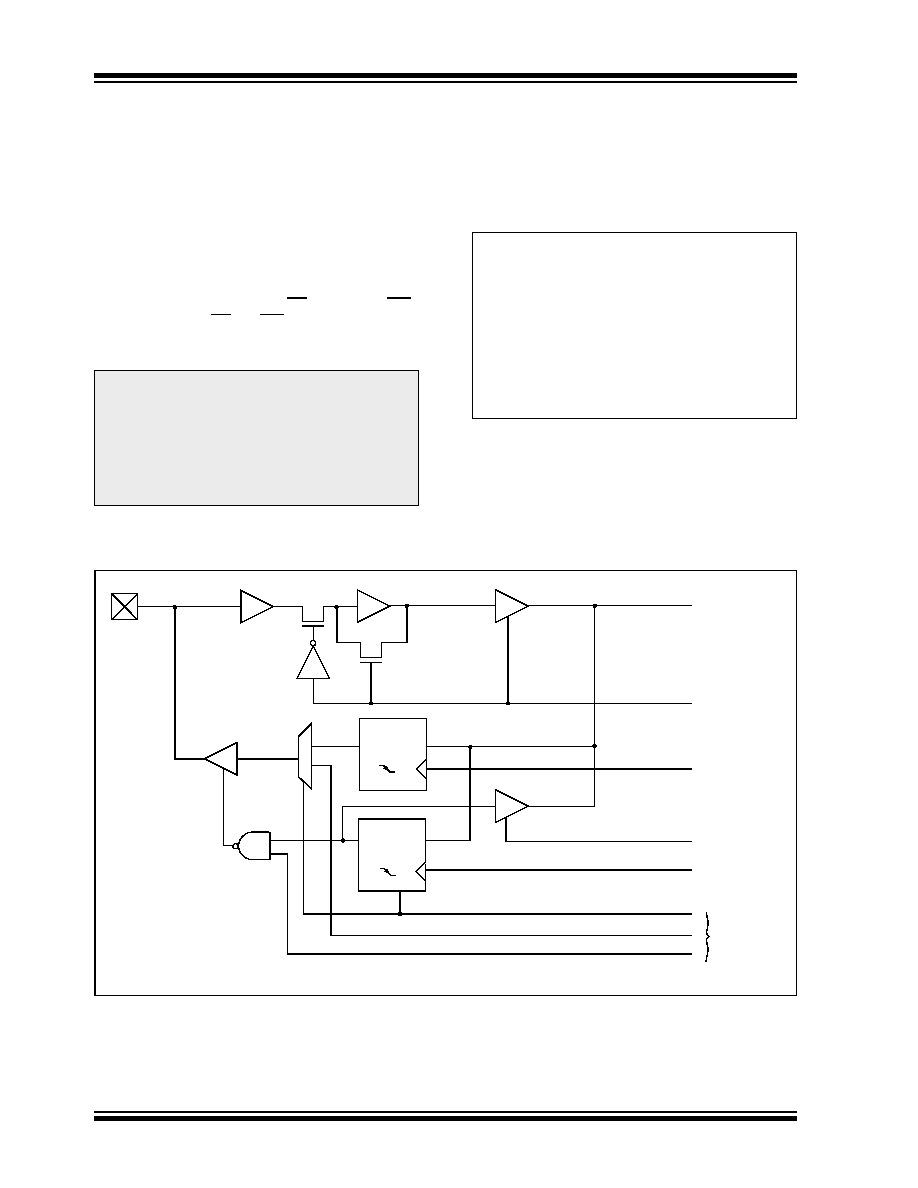
FIGURE 10-11:
BLOCK DIAGRAM OF RE2:RE0 (IN I/O PORT MODE)
Note:
Three pins of this port are configured as
the system bus when the device’s configu-
ration bits are selected to Microprocessor
or Extended Microcontroller modes. The
other pin is a general purpose I/O or
Capture4 pin. In the two other micro-
controller modes, RE2:RE0 are general
purpose I/O pins.
MOVLB
1
; Select Bank 1
CLRF
PORTE, F
; Initialize PORTE data
; latches before setting
; the data direction
; register
MOVLW
0x03
; Value used to initialize
; data direction
MOVWF
DDRE
; Set RE<1:0> as inputs
; RE<3:2> as outputs
; RE<7:4> are always
; read as ’0’
Note: I/O pins have protection diodes to VDD and VSS.
Q
D
CK
TTL
0
1
Q
D
CK
R
S
Input
Buffer
Port
Data
Data Bus
RD_PORTE
WR_PORTE
RD_DDRE
WR_DDRE
EX_EN
CNTL
DRV_SYS
System Bus
Control
相关PDF资料 |
PDF描述 |
|---|---|
| ADG801BRM-REEL | IC SWITCH SPST 8MSOP |
| PIC17C756AT-33/PT | IC MCU OTP 16KX16 A/D PWM 64TQFP |
| ADG711BRU-REEL | IC SWITCH QUAD SPST 16TSSOP |
| V375C3V3M75BL | CONVERTER MOD DC/DC 3.3V 75W |
| RPER71H102K2P1A03B | CAP CER 1000PF 50V 10% RADIAL |
相关代理商/技术参数 |
参数描述 |
|---|---|
| PIC17C752-33/L | 功能描述:8位微控制器 -MCU 16KB 678 RAM 50 I/O RoHS:否 制造商:Silicon Labs 核心:8051 处理器系列:C8051F39x 数据总线宽度:8 bit 最大时钟频率:50 MHz 程序存储器大小:16 KB 数据 RAM 大小:1 KB 片上 ADC:Yes 工作电源电压:1.8 V to 3.6 V 工作温度范围:- 40 C to + 105 C 封装 / 箱体:QFN-20 安装风格:SMD/SMT |
| PIC17C752-33/PT | 功能描述:8位微控制器 -MCU 16KB 678 RAM 50 I/O RoHS:否 制造商:Silicon Labs 核心:8051 处理器系列:C8051F39x 数据总线宽度:8 bit 最大时钟频率:50 MHz 程序存储器大小:16 KB 数据 RAM 大小:1 KB 片上 ADC:Yes 工作电源电压:1.8 V to 3.6 V 工作温度范围:- 40 C to + 105 C 封装 / 箱体:QFN-20 安装风格:SMD/SMT |
| PIC17C752-33E/L | 功能描述:8位微控制器 -MCU 16KB 678 RAM 50 I/O RoHS:否 制造商:Silicon Labs 核心:8051 处理器系列:C8051F39x 数据总线宽度:8 bit 最大时钟频率:50 MHz 程序存储器大小:16 KB 数据 RAM 大小:1 KB 片上 ADC:Yes 工作电源电压:1.8 V to 3.6 V 工作温度范围:- 40 C to + 105 C 封装 / 箱体:QFN-20 安装风格:SMD/SMT |
| PIC17C752-33E/PT | 功能描述:8位微控制器 -MCU 16KB 678 RAM 50 I/O RoHS:否 制造商:Silicon Labs 核心:8051 处理器系列:C8051F39x 数据总线宽度:8 bit 最大时钟频率:50 MHz 程序存储器大小:16 KB 数据 RAM 大小:1 KB 片上 ADC:Yes 工作电源电压:1.8 V to 3.6 V 工作温度范围:- 40 C to + 105 C 封装 / 箱体:QFN-20 安装风格:SMD/SMT |
| PIC17C752-33I/L | 功能描述:8位微控制器 -MCU 16KB 678 RAM 50 I/O RoHS:否 制造商:Silicon Labs 核心:8051 处理器系列:C8051F39x 数据总线宽度:8 bit 最大时钟频率:50 MHz 程序存储器大小:16 KB 数据 RAM 大小:1 KB 片上 ADC:Yes 工作电源电压:1.8 V to 3.6 V 工作温度范围:- 40 C to + 105 C 封装 / 箱体:QFN-20 安装风格:SMD/SMT |
发布紧急采购,3分钟左右您将得到回复。