- 您现在的位置:买卖IC网 > PDF目录190063 > PIC17C766T-33E/L 8-BIT, OTPROM, 33 MHz, RISC MICROCONTROLLER, PQCC84 PDF资料下载
参数资料
| 型号: | PIC17C766T-33E/L |
| 元件分类: | 微控制器/微处理器 |
| 英文描述: | 8-BIT, OTPROM, 33 MHz, RISC MICROCONTROLLER, PQCC84 |
| 封装: | PLASTIC, MO-047, LCC-84 |
| 文件页数: | 30/303页 |
| 文件大小: | 5350K |
| 代理商: | PIC17C766T-33E/L |
第1页第2页第3页第4页第5页第6页第7页第8页第9页第10页第11页第12页第13页第14页第15页第16页第17页第18页第19页第20页第21页第22页第23页第24页第25页第26页第27页第28页第29页当前第30页第31页第32页第33页第34页第35页第36页第37页第38页第39页第40页第41页第42页第43页第44页第45页第46页第47页第48页第49页第50页第51页第52页第53页第54页第55页第56页第57页第58页第59页第60页第61页第62页第63页第64页第65页第66页第67页第68页第69页第70页第71页第72页第73页第74页第75页第76页第77页第78页第79页第80页第81页第82页第83页第84页第85页第86页第87页第88页第89页第90页第91页第92页第93页第94页第95页第96页第97页第98页第99页第100页第101页第102页第103页第104页第105页第106页第107页第108页第109页第110页第111页第112页第113页第114页第115页第116页第117页第118页第119页第120页第121页第122页第123页第124页第125页第126页第127页第128页第129页第130页第131页第132页第133页第134页第135页第136页第137页第138页第139页第140页第141页第142页第143页第144页第145页第146页第147页第148页第149页第150页第151页第152页第153页第154页第155页第156页第157页第158页第159页第160页第161页第162页第163页第164页第165页第166页第167页第168页第169页第170页第171页第172页第173页第174页第175页第176页第177页第178页第179页第180页第181页第182页第183页第184页第185页第186页第187页第188页第189页第190页第191页第192页第193页第194页第195页第196页第197页第198页第199页第200页第201页第202页第203页第204页第205页第206页第207页第208页第209页第210页第211页第212页第213页第214页第215页第216页第217页第218页第219页第220页第221页第222页第223页第224页第225页第226页第227页第228页第229页第230页第231页第232页第233页第234页第235页第236页第237页第238页第239页第240页第241页第242页第243页第244页第245页第246页第247页第248页第249页第250页第251页第252页第253页第254页第255页第256页第257页第258页第259页第260页第261页第262页第263页第264页第265页第266页第267页第268页第269页第270页第271页第272页第273页第274页第275页第276页第277页第278页第279页第280页第281页第282页第283页第284页第285页第286页第287页第288页第289页第290页第291页第292页第293页第294页第295页第296页第297页第298页第299页第300页第301页第302页第303页
2000 Microchip Technology Inc.
DS30289B-page 125
PIC17C7XX
14.2.2
USART ASYNCHRONOUS
RECEIVER
The receiver block diagram is shown in Figure 14-2.
The data comes in the RX/DT pin and drives the data
recovery block. The data recovery block is actually a
high speed shifter operating at 16 times the baud rate,
whereas the main receive serial shifter operates at the
bit rate or at FOSC.
Once Asynchronous mode is selected, reception is
enabled by setting bit CREN (RCSTA<4>).
The heart of the receiver is the receive (serial) shift reg-
ister (RSR). After sampling the STOP bit, the received
data in the RSR is transferred to the RCREG (if it is
empty). If the transfer is complete, the interrupt bit,
RCIF, is set. The actual interrupt can be enabled/
disabled by setting/clearing the RCIE bit. RCIF is a
read only bit which is cleared by the hardware. It is
cleared when RCREG has been read and is empty.
RCREG is a double buffered register (i.e., it is a two-
deep FIFO). It is possible for two bytes of data to be
received and transferred to the RCREG FIFO and a
third byte begin shifting to the RSR. On detection of the
STOP bit of the third byte, if the RCREG is still full, then
the overrun error bit, OERR (RCSTA<1>) will be set.
The word in the RSR will be lost. RCREG can be read
twice to retrieve the two bytes in the FIFO. The OERR
bit has to be cleared in software which is done by reset-
ting the receive logic (CREN is set). If the OERR bit is
set, transfers from the RSR to RCREG are inhibited, so
it is essential to clear the OERR bit if it is set. The fram-
ing error bit FERR (RCSTA<2>) is set if a STOP bit is
not detected.
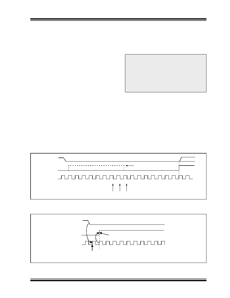
14.2.3
SAMPLING
The data on the RX/DT pin is sampled three times by a
majority detect circuit to determine if a high or a low
level is present at the RX/DT pin. The sampling is done
on the seventh, eighth and ninth falling edges of a x16
clock (Figure 14-5).
The x16 clock is a free running clock and the three
sample points occur at a frequency of every 16 falling
edges.
FIGURE 14-5:
RX PIN SAMPLING SCHEME
FIGURE 14-6:
START BIT DETECT
Note:
The FERR and the 9th receive bit are buff-
ered the same way as the receive data.
Reading the RCREG register will allow the
RX9D and FERR bits to be loaded with val-
ues for the next received data. Therefore,
it is essential for the user to read the
RCSTA register before reading RCREG, in
order not to lose the old FERR and RX9D
information.
RX
Baud CLK
x16 CLK
START bit
Bit0
Samples
1
2
3
4
5
6
7
8
9
10
11
12
13
14
15
16
1
2
3
Baud CLK for all but START bit
(RX/DT pin)
RX
x16 CLK
Q2, Q4 CLK
START bit
(RX/DT pin)
First rising edge of x16 clock after RX pin goes low
RX sampled low
相关PDF资料 |
PDF描述 |
|---|---|
| PIC18C242-I/SO | 8-BIT, OTPROM, 40 MHz, RISC MICROCONTROLLER, PDSO28 |
| PIC18C442-E/L | 8-BIT, OTPROM, 40 MHz, RISC MICROCONTROLLER, PQCC44 |
| PIC18F2515 | PIC18FX515/X610 Product Brief |
| PIC18F2539 | PIC18F2539 Motor Control Evaluation Kit |
| PIC18F4439 | PIC18XXX Tools Quick Chart |
相关代理商/技术参数 |
参数描述 |
|---|---|
| PIC17C766T-33I/L | 功能描述:8位微控制器 -MCU 33MHz 16K EPRM RoHS:否 制造商:Silicon Labs 核心:8051 处理器系列:C8051F39x 数据总线宽度:8 bit 最大时钟频率:50 MHz 程序存储器大小:16 KB 数据 RAM 大小:1 KB 片上 ADC:Yes 工作电源电压:1.8 V to 3.6 V 工作温度范围:- 40 C to + 105 C 封装 / 箱体:QFN-20 安装风格:SMD/SMT |
| PIC17C766T-33I/PT | 功能描述:8位微控制器 -MCU 32KB 902 RAM 66 I/O RoHS:否 制造商:Silicon Labs 核心:8051 处理器系列:C8051F39x 数据总线宽度:8 bit 最大时钟频率:50 MHz 程序存储器大小:16 KB 数据 RAM 大小:1 KB 片上 ADC:Yes 工作电源电压:1.8 V to 3.6 V 工作温度范围:- 40 C to + 105 C 封装 / 箱体:QFN-20 安装风格:SMD/SMT |
| PIC17LC42A-08/L | 功能描述:8位微控制器 -MCU 4KB 232 RAM 33 I/O RoHS:否 制造商:Silicon Labs 核心:8051 处理器系列:C8051F39x 数据总线宽度:8 bit 最大时钟频率:50 MHz 程序存储器大小:16 KB 数据 RAM 大小:1 KB 片上 ADC:Yes 工作电源电压:1.8 V to 3.6 V 工作温度范围:- 40 C to + 105 C 封装 / 箱体:QFN-20 安装风格:SMD/SMT |
| PIC17LC42A-08/P | 功能描述:8位微控制器 -MCU 4KB 232 RAM 33 I/O RoHS:否 制造商:Silicon Labs 核心:8051 处理器系列:C8051F39x 数据总线宽度:8 bit 最大时钟频率:50 MHz 程序存储器大小:16 KB 数据 RAM 大小:1 KB 片上 ADC:Yes 工作电源电压:1.8 V to 3.6 V 工作温度范围:- 40 C to + 105 C 封装 / 箱体:QFN-20 安装风格:SMD/SMT |
| PIC17LC42A-08/PQ | 功能描述:8位微控制器 -MCU 4KB 232 RAM 33 I/O RoHS:否 制造商:Silicon Labs 核心:8051 处理器系列:C8051F39x 数据总线宽度:8 bit 最大时钟频率:50 MHz 程序存储器大小:16 KB 数据 RAM 大小:1 KB 片上 ADC:Yes 工作电源电压:1.8 V to 3.6 V 工作温度范围:- 40 C to + 105 C 封装 / 箱体:QFN-20 安装风格:SMD/SMT |
发布紧急采购,3分钟左右您将得到回复。