- 您现在的位置:买卖IC网 > PDF目录3873 > PIC18F13K50-I/P (Microchip Technology)IC PIC MCU FLASH 4KX16 20-PDIP PDF资料下载
参数资料
| 型号: | PIC18F13K50-I/P |
| 厂商: | Microchip Technology |
| 文件页数: | 239/285页 |
| 文件大小: | 0K |
| 描述: | IC PIC MCU FLASH 4KX16 20-PDIP |
| 产品培训模块: | XLP Deep Sleep Mode 8-bit PIC® Microcontroller Portfolio |
| 标准包装: | 22 |
| 系列: | PIC® XLP™ 18F |
| 核心处理器: | PIC |
| 芯体尺寸: | 8-位 |
| 速度: | 48MHz |
| 连通性: | I²C,SPI,UART/USART,USB |
| 外围设备: | 欠压检测/复位,POR,PWM,WDT |
| 输入/输出数: | 14 |
| 程序存储器容量: | 8KB(4K x 16) |
| 程序存储器类型: | 闪存 |
| EEPROM 大小: | 256 x 8 |
| RAM 容量: | 512 x 8 |
| 电压 - 电源 (Vcc/Vdd): | 1.8 V ~ 5.5 V |
| 数据转换器: | A/D 11x10b |
| 振荡器型: | 内部 |
| 工作温度: | -40°C ~ 85°C |
| 封装/外壳: | 20-DIP(0.300",7.62mm) |
| 包装: | 管件 |
| 产品目录页面: | 642 (CN2011-ZH PDF) |
| 配用: | DV164126-ND - KIT DEVELOPMENT USB W/PICKIT 2 DM164127-ND - KIT DEVELOPMENT USB 18F14/13K50 AC164112-ND - VOLTAGE LIMITER MPLAB ICD2 VPP |
第1页第2页第3页第4页第5页第6页第7页第8页第9页第10页第11页第12页第13页第14页第15页第16页第17页第18页第19页第20页第21页第22页第23页第24页第25页第26页第27页第28页第29页第30页第31页第32页第33页第34页第35页第36页第37页第38页第39页第40页第41页第42页第43页第44页第45页第46页第47页第48页第49页第50页第51页第52页第53页第54页第55页第56页第57页第58页第59页第60页第61页第62页第63页第64页第65页第66页第67页第68页第69页第70页第71页第72页第73页第74页第75页第76页第77页第78页第79页第80页第81页第82页第83页第84页第85页第86页第87页第88页第89页第90页第91页第92页第93页第94页第95页第96页第97页第98页第99页第100页第101页第102页第103页第104页第105页第106页第107页第108页第109页第110页第111页第112页第113页第114页第115页第116页第117页第118页第119页第120页第121页第122页第123页第124页第125页第126页第127页第128页第129页第130页第131页第132页第133页第134页第135页第136页第137页第138页第139页第140页第141页第142页第143页第144页第145页第146页第147页第148页第149页第150页第151页第152页第153页第154页第155页第156页第157页第158页第159页第160页第161页第162页第163页第164页第165页第166页第167页第168页第169页第170页第171页第172页第173页第174页第175页第176页第177页第178页第179页第180页第181页第182页第183页第184页第185页第186页第187页第188页第189页第190页第191页第192页第193页第194页第195页第196页第197页第198页第199页第200页第201页第202页第203页第204页第205页第206页第207页第208页第209页第210页第211页第212页第213页第214页第215页第216页第217页第218页第219页第220页第221页第222页第223页第224页第225页第226页第227页第228页第229页第230页第231页第232页第233页第234页第235页第236页第237页第238页当前第239页第240页第241页第242页第243页第244页第245页第246页第247页第248页第249页第250页第251页第252页第253页第254页第255页第256页第257页第258页第259页第260页第261页第262页第263页第264页第265页第266页第267页第268页第269页第270页第271页第272页第273页第274页第275页第276页第277页第278页第279页第280页第281页第282页第283页第284页第285页
2010 Microchip Technology Inc.
Preliminary
DS41350E-page 57
PIC18F1XK50/PIC18LF1XK50
4.5
Writing to Flash Program Memory
The programming block size is 8 or 16 bytes,
depending on the device (See Table 4-1). Word or byte
programming is not supported.
Table writes are used internally to load the holding
registers needed to program the Flash memory. There
are only as many holding registers as there are bytes
in a write block (See Table 4-1).
Since the Table Latch (TABLAT) is only a single byte,
the TBLWT instruction may need to be executed 8, or 16
times, depending on the device, for each programming
operation. All of the table write operations will essen-
tially be short writes because only the holding registers
are written. After all the holding registers have been
written, the programming operation of that block of
memory is started by configuring the EECON1 register
for a program memory write and performing the long
write sequence.
The long write is necessary for programming the inter-
nal Flash. Instruction execution is halted during a long
write cycle. The long write will be terminated by the
internal programming timer.
The EEPROM on-chip timer controls the write time.
The write/erase voltages are generated by an on-chip
charge pump, rated to operate over the voltage range
of the device.
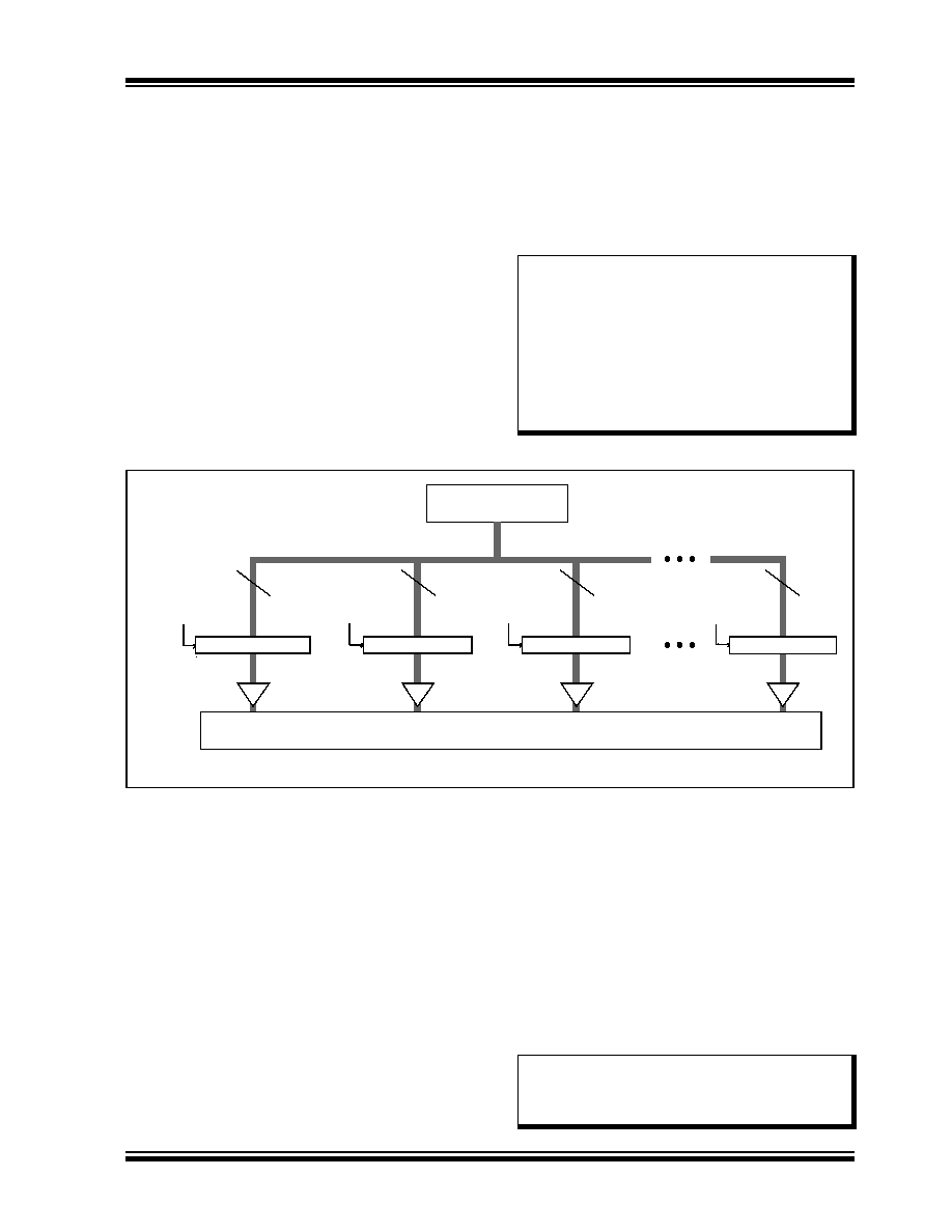
FIGURE 4-5:
TABLE WRITES TO FLASH PROGRAM MEMORY
4.5.1
FLASH PROGRAM MEMORY WRITE
SEQUENCE
The sequence of events for programming an internal
program memory location should be:
1.
Read 64 bytes into RAM.
2.
Update data values in RAM as necessary.
3.
Load Table Pointer register with address being
erased.
4.
Execute the block erase procedure.
5.
Load Table Pointer register with address of first
byte being written.
6.
Write the 8 or 16-byte block into the holding
registers with auto-increment.
7.
Set the EECON1 register for the write operation:
set EEPGD bit to point to program memory;
clear the CFGS bit to access program memory;
set WREN to enable byte writes.
8.
Disable interrupts.
9.
Write 55h to EECON2.
10. Write 0AAh to EECON2.
11. Set the WR bit. This will begin the write cycle.
12. The CPU will stall for duration of the write (about
2 ms using internal timer).
13. Re-enable interrupts.
14. Repeat steps 6 to 13 for each block until all 64
bytes are written.
15. Verify the memory (table read).
This procedure will require about 6 ms to update each
write block of memory. An example of the required code
is given in Example 4-3.
Note:
The default value of the holding registers on
device Resets and after write operations is
FFh. A write of FFh to a holding register
does not modify that byte. This means that
individual bytes of program memory may
be modified, provided that the change does
not attempt to change any bit from a ‘0’ to a
‘1’. When modifying individual bytes, it is
not necessary to load all holding registers
before executing a long write operation.
TABLAT
TBLPTR = xxxxYY
(1)
TBLPTR = xxxx01
TBLPTR = xxxx00
Write Register
TBLPTR = xxxx02
Program Memory
Holding Register
8
Note 1: YY = x7, xF, or 1F for 8, 16 or 32 byte write blocks, respectively.
Note:
Before setting the WR bit, the Table
Pointer address needs to be within the
intended address range of the bytes in the
holding registers.
相关PDF资料 |
PDF描述 |
|---|---|
| PIC16CR76T-I/SO | IC PIC MCU 8KX14 28SOIC |
| PIC18LF24K22-I/MV | IC PIC MCU 16KB FLASH 28UQFN |
| PIC18LF24K22-I/ML | IC PIC MCU 16KB FLASH 28QFN |
| PIC16CR76T-I/ML | IC PIC MCU 8KX14 28QFN |
| PIC16F627-04/P | IC MCU FLASH 1KX14 COMP 18DIP |
相关代理商/技术参数 |
参数描述 |
|---|---|
| PIC18F13K50T-I/SO | 功能描述:8位微控制器 -MCU 8KB Flash 512 RAM 15 I/O 10-B ADC USB 2.0 RoHS:否 制造商:Silicon Labs 核心:8051 处理器系列:C8051F39x 数据总线宽度:8 bit 最大时钟频率:50 MHz 程序存储器大小:16 KB 数据 RAM 大小:1 KB 片上 ADC:Yes 工作电源电压:1.8 V to 3.6 V 工作温度范围:- 40 C to + 105 C 封装 / 箱体:QFN-20 安装风格:SMD/SMT |
| PIC18F13K50T-I/SS | 功能描述:8位微控制器 -MCU 8KB Flash 512 RAM 15 I/O 10-B ADC USB 2.0 RoHS:否 制造商:Silicon Labs 核心:8051 处理器系列:C8051F39x 数据总线宽度:8 bit 最大时钟频率:50 MHz 程序存储器大小:16 KB 数据 RAM 大小:1 KB 片上 ADC:Yes 工作电源电压:1.8 V to 3.6 V 工作温度范围:- 40 C to + 105 C 封装 / 箱体:QFN-20 安装风格:SMD/SMT |
| PIC18F14K22-E/ML | 功能描述:8位微控制器 -MCU 16KBFlash 512byteRAM 256bytesEEPROM RoHS:否 制造商:Silicon Labs 核心:8051 处理器系列:C8051F39x 数据总线宽度:8 bit 最大时钟频率:50 MHz 程序存储器大小:16 KB 数据 RAM 大小:1 KB 片上 ADC:Yes 工作电源电压:1.8 V to 3.6 V 工作温度范围:- 40 C to + 105 C 封装 / 箱体:QFN-20 安装风格:SMD/SMT |
| PIC18F14K22-E/P | 功能描述:8位微控制器 -MCU 16KBFlash 512byteRAM 256bytesEEPROM RoHS:否 制造商:Silicon Labs 核心:8051 处理器系列:C8051F39x 数据总线宽度:8 bit 最大时钟频率:50 MHz 程序存储器大小:16 KB 数据 RAM 大小:1 KB 片上 ADC:Yes 工作电源电压:1.8 V to 3.6 V 工作温度范围:- 40 C to + 105 C 封装 / 箱体:QFN-20 安装风格:SMD/SMT |
| PIC18F14K22-E/SO | 功能描述:8位微控制器 -MCU 16KBFlash 512byteRAM 256bytesEEPROM RoHS:否 制造商:Silicon Labs 核心:8051 处理器系列:C8051F39x 数据总线宽度:8 bit 最大时钟频率:50 MHz 程序存储器大小:16 KB 数据 RAM 大小:1 KB 片上 ADC:Yes 工作电源电压:1.8 V to 3.6 V 工作温度范围:- 40 C to + 105 C 封装 / 箱体:QFN-20 安装风格:SMD/SMT |
发布紧急采购,3分钟左右您将得到回复。