- 您现在的位置:买卖IC网 > PDF目录11402 > PIC18F2423-E/ML (Microchip Technology)IC PIC MCU FLASH 8KX16 28QFN PDF资料下载
参数资料
| 型号: | PIC18F2423-E/ML |
| 厂商: | Microchip Technology |
| 文件页数: | 21/54页 |
| 文件大小: | 0K |
| 描述: | IC PIC MCU FLASH 8KX16 28QFN |
| 产品培训模块: | Asynchronous Stimulus |
| 标准包装: | 61 |
| 系列: | PIC® 18F |
| 核心处理器: | PIC |
| 芯体尺寸: | 8-位 |
| 速度: | 40MHz |
| 连通性: | I²C,SPI,UART/USART |
| 外围设备: | 欠压检测/复位,HLVD,POR,PWM,WDT |
| 输入/输出数: | 25 |
| 程序存储器容量: | 16KB(8K x 16) |
| 程序存储器类型: | 闪存 |
| EEPROM 大小: | 256 x 8 |
| RAM 容量: | 768 x 8 |
| 电压 - 电源 (Vcc/Vdd): | 4.2 V ~ 5.5 V |
| 数据转换器: | A/D 10x12b |
| 振荡器型: | 内部 |
| 工作温度: | -40°C ~ 125°C |
| 封装/外壳: | 28-VQFN 裸露焊盘 |
| 包装: | 管件 |
第1页第2页第3页第4页第5页第6页第7页第8页第9页第10页第11页第12页第13页第14页第15页第16页第17页第18页第19页第20页当前第21页第22页第23页第24页第25页第26页第27页第28页第29页第30页第31页第32页第33页第34页第35页第36页第37页第38页第39页第40页第41页第42页第43页第44页第45页第46页第47页第48页第49页第50页第51页第52页第53页第54页
PIC18F2423/2523/4423/4523
DS39755C-page 28
2009 Microchip Technology Inc.
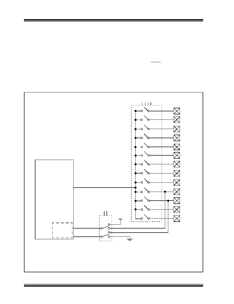
The analog reference voltage is software selectable to
either the device’s positive and negative supply voltage
(VDD and VSS), or the voltage level on the RA3/AN3/
VREF+ and RA2/AN2/VREF-/CVREF pins.
The A/D Converter has a unique feature of being able
to operate while the device is in Sleep mode. To oper-
ate in Sleep, the A/D conversion clock must be derived
from the A/D’s internal RC oscillator.
The output of the sample and hold is the input into the
converter, which generates the result via successive
approximation.
A device Reset forces all registers to their Reset state.
This forces the A/D module to be turned off and any
conversion in progress is aborted.
Each port pin associated with the A/D Converter can be
configured as an analog input or as a digital I/O. The
ADRESH and ADRESL registers contain the result of
the A/D conversion. When the A/D conversion is com-
plete, the result is loaded into the ADRESH:ADRESL
register pair, the GO/DONE bit (ADCON0<1>) is cleared
and A/D Interrupt Flag bit, ADIF, is set.
The block diagram of the A/D module is shown in
FIGURE 2-1:
A/D BLOCK DIAGRAM
(Input Voltage)
VAIN
VREF+
Reference
Voltage
VDD(2)
VCFG<1:0>
CHS<3:0>
AN7(1)
AN6(1)
AN5(1)
AN4
AN3
AN2
AN1
AN0
0111
0110
0101
0100
0011
0010
0001
0000
12-Bit
A/D
VREF-
VSS(2)
Converter
AN12
AN11
AN10
AN9
AN8
1100
1011
1010
1001
1000
Note 1: Channels, AN5 through AN7, are not available on PIC18F2423/2523 devices.
2: I/O pins have diode protection to VDD and VSS.
0X
1X
X
1
X
0
相关PDF资料 |
PDF描述 |
|---|---|
| DSPIC30F3012-20E/ML | IC DSPIC MCU/DSP 24K 44QFN |
| PIC18LF2455T-I/SO | IC PIC MCU FLASH 12KX16 28SOIC |
| FGG.0B.304.CLAD52Z | CONN PLUG 4POS STRGHT PIN SOLDER |
| FGG.0B.304.CLAD31Z | CONN PLUG 4POS STRGHT PIN SOLDER |
| VE-24Y-IY | CONVERTER MOD DC/DC 3.3V 33W |
相关代理商/技术参数 |
参数描述 |
|---|---|
| PIC18F2423-I/ML | 功能描述:8位微控制器 -MCU 16KB FL 768bytes- RAM 25I/O RoHS:否 制造商:Silicon Labs 核心:8051 处理器系列:C8051F39x 数据总线宽度:8 bit 最大时钟频率:50 MHz 程序存储器大小:16 KB 数据 RAM 大小:1 KB 片上 ADC:Yes 工作电源电压:1.8 V to 3.6 V 工作温度范围:- 40 C to + 105 C 封装 / 箱体:QFN-20 安装风格:SMD/SMT |
| PIC18F2423-I/SO | 功能描述:8位微控制器 -MCU 16KB FL 768bytes- RAM 25I/O RoHS:否 制造商:Silicon Labs 核心:8051 处理器系列:C8051F39x 数据总线宽度:8 bit 最大时钟频率:50 MHz 程序存储器大小:16 KB 数据 RAM 大小:1 KB 片上 ADC:Yes 工作电源电压:1.8 V to 3.6 V 工作温度范围:- 40 C to + 105 C 封装 / 箱体:QFN-20 安装风格:SMD/SMT |
| PIC18F2423-I/SO | 制造商:Microchip Technology Inc 功能描述:8-Bit Microcontroller IC |
| PIC18F2423-I/SP | 功能描述:8位微控制器 -MCU 16KB FL 768bytes- RAM 25I/O RoHS:否 制造商:Silicon Labs 核心:8051 处理器系列:C8051F39x 数据总线宽度:8 bit 最大时钟频率:50 MHz 程序存储器大小:16 KB 数据 RAM 大小:1 KB 片上 ADC:Yes 工作电源电压:1.8 V to 3.6 V 工作温度范围:- 40 C to + 105 C 封装 / 箱体:QFN-20 安装风格:SMD/SMT |
| PIC18F2423T-I/ML | 功能描述:8位微控制器 -MCU 16KB FL 768bytes- RAM 25I/O RoHS:否 制造商:Silicon Labs 核心:8051 处理器系列:C8051F39x 数据总线宽度:8 bit 最大时钟频率:50 MHz 程序存储器大小:16 KB 数据 RAM 大小:1 KB 片上 ADC:Yes 工作电源电压:1.8 V to 3.6 V 工作温度范围:- 40 C to + 105 C 封装 / 箱体:QFN-20 安装风格:SMD/SMT |
发布紧急采购,3分钟左右您将得到回复。