- 您现在的位置:买卖IC网 > PDF目录11427 > PIC18F2423T-I/SO (Microchip Technology)IC PIC MCU FLASH 8KX16 28SOIC PDF资料下载
参数资料
| 型号: | PIC18F2423T-I/SO |
| 厂商: | Microchip Technology |
| 文件页数: | 25/54页 |
| 文件大小: | 0K |
| 描述: | IC PIC MCU FLASH 8KX16 28SOIC |
| 产品培训模块: | Asynchronous Stimulus |
| 标准包装: | 1,600 |
| 系列: | PIC® 18F |
| 核心处理器: | PIC |
| 芯体尺寸: | 8-位 |
| 速度: | 40MHz |
| 连通性: | I²C,SPI,UART/USART |
| 外围设备: | 欠压检测/复位,HLVD,POR,PWM,WDT |
| 输入/输出数: | 25 |
| 程序存储器容量: | 16KB(8K x 16) |
| 程序存储器类型: | 闪存 |
| EEPROM 大小: | 256 x 8 |
| RAM 容量: | 768 x 8 |
| 电压 - 电源 (Vcc/Vdd): | 4.2 V ~ 5.5 V |
| 数据转换器: | A/D 10x12b |
| 振荡器型: | 内部 |
| 工作温度: | -40°C ~ 85°C |
| 封装/外壳: | 28-SOIC(0.295",7.50mm 宽) |
| 包装: | 带卷 (TR) |
| 其它名称: | PIC18F2423T-I/SOTR |
第1页第2页第3页第4页第5页第6页第7页第8页第9页第10页第11页第12页第13页第14页第15页第16页第17页第18页第19页第20页第21页第22页第23页第24页当前第25页第26页第27页第28页第29页第30页第31页第32页第33页第34页第35页第36页第37页第38页第39页第40页第41页第42页第43页第44页第45页第46页第47页第48页第49页第50页第51页第52页第53页第54页
2009 Microchip Technology Inc.
DS39755C-page 31
PIC18F2423/2523/4423/4523
2.2
Selecting and Configuring
Acquisition Time
The ADCON2 register allows the user to select an
acquisition time that occurs each time the GO/DONE
bit is set. It also gives users the option of having an
automatically determined acquisition time.
Acquisition time may be set with the ACQT<2:0> bits
(ADCON2<5:3>), which provide a range of 2 to 20 TAD.
When the GO/DONE bit is set, the A/D module con-
tinues to sample the input for the selected acquisition
time, then automatically begins a conversion. Since the
acquisition time is programmed, there may be no need
to wait for an acquisition time between selecting a
channel and setting the GO/DONE bit.
Manual
acquisition
time
is
selected
when
ACQT<2:0> = 000. When the GO/DONE bit is set,
sampling is stopped and a conversion begins. The user
is responsible for ensuring the required acquisition time
has passed between selecting the desired input
channel and setting the GO/DONE bit. This option is
also the default Reset state of the ACQT<2:0> bits and
is compatible with devices that do not offer
programmable acquisition times.
In either case, when the conversion is completed, the
GO/DONE bit is cleared, the ADIF flag is set and the
A/D begins sampling the currently selected channel
again. If an acquisition time is programmed, there is
nothing to indicate if the acquisition time has ended or
if the conversion has begun.
2.3
Selecting the A/D Conversion
Clock
The A/D conversion time per bit is defined as TAD. The
A/D conversion requires 13 TAD per 12-bit conversion.
The source of the A/D conversion clock is software
selectable.
There are seven possible options for TAD:
For correct A/D conversions, the A/D conversion clock
(TAD) must be as short as possible, but greater than the
the device operating frequencies and the A/D clock
source selected.
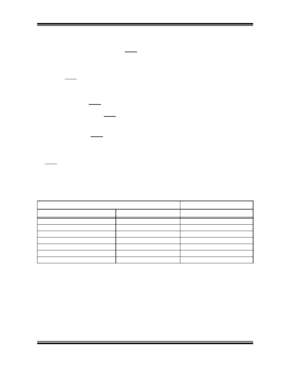
TABLE 2-2:
TAD vs. DEVICE OPERATING FREQUENCIES
2 TOSC
32 TOSC
4 TOSC
64 TOSC
8 TOSC
Internal RC Oscillator
16 TOSC
A/D Clock Source (TAD)
Assumes TAD Min. = 0.8
μs
Operation
ADCS<2:0>
Maximum FOSC
2 TOSC
000
2.50 MHz
4 TOSC
100
5.00 MHz
8 TOSC
001
10.00 MHz
16 TOSC
101
20.00 MHz
32 TOSC
010
40.00 MHz
64 TOSC
110
40.00 MHz
RC(2)
x11
1.00 MHz(1)
Note 1:
The RC source has a typical TAD time of 2.5
μs.
2:
For device frequencies above 1 MHz, the device must be in Sleep for the entire conversion or a FOSC
divider should be used instead; otherwise, the A/D accuracy specification may not be met.
相关PDF资料 |
PDF描述 |
|---|---|
| PIC16C715T-20I/SS | IC MCU OTP 2KX14 A/D 20SSOP |
| DSPIC30F3010T-30I/SO | IC DSPIC MCU/DSP 24K 28SOIC |
| PIC18F66K22-E/MR | IC MCU PIC 64K FLASH XLP 64QFN |
| PIC18F65K80-E/MR | MCU PIC 32KB FLASH ECAN 64QFN |
| DSPIC33FJ16GS404-E/PT | IC DSPIC MCU/DSP 16K 44-TQFP |
相关代理商/技术参数 |
参数描述 |
|---|---|
| PIC18F242-E/SO | 功能描述:8位微控制器 -MCU 16KB 768 RAM 23I/O RoHS:否 制造商:Silicon Labs 核心:8051 处理器系列:C8051F39x 数据总线宽度:8 bit 最大时钟频率:50 MHz 程序存储器大小:16 KB 数据 RAM 大小:1 KB 片上 ADC:Yes 工作电源电压:1.8 V to 3.6 V 工作温度范围:- 40 C to + 105 C 封装 / 箱体:QFN-20 安装风格:SMD/SMT |
| PIC18F242-E/SP | 功能描述:8位微控制器 -MCU 16KB 768 RAM 23I/O RoHS:否 制造商:Silicon Labs 核心:8051 处理器系列:C8051F39x 数据总线宽度:8 bit 最大时钟频率:50 MHz 程序存储器大小:16 KB 数据 RAM 大小:1 KB 片上 ADC:Yes 工作电源电压:1.8 V to 3.6 V 工作温度范围:- 40 C to + 105 C 封装 / 箱体:QFN-20 安装风格:SMD/SMT |
| PIC18F242-I/SO | 功能描述:8位微控制器 -MCU 16KB 768 RAM 23I/O RoHS:否 制造商:Silicon Labs 核心:8051 处理器系列:C8051F39x 数据总线宽度:8 bit 最大时钟频率:50 MHz 程序存储器大小:16 KB 数据 RAM 大小:1 KB 片上 ADC:Yes 工作电源电压:1.8 V to 3.6 V 工作温度范围:- 40 C to + 105 C 封装 / 箱体:QFN-20 安装风格:SMD/SMT |
| PIC18F242-I/SO | 制造商:Microchip Technology Inc 功能描述:8BIT FLASH MCU SMD 18F242 SOIC28 |
| PIC18F242-I/SP | 功能描述:8位微控制器 -MCU 16KB 768 RAM 23I/O RoHS:否 制造商:Silicon Labs 核心:8051 处理器系列:C8051F39x 数据总线宽度:8 bit 最大时钟频率:50 MHz 程序存储器大小:16 KB 数据 RAM 大小:1 KB 片上 ADC:Yes 工作电源电压:1.8 V to 3.6 V 工作温度范围:- 40 C to + 105 C 封装 / 箱体:QFN-20 安装风格:SMD/SMT |
发布紧急采购,3分钟左右您将得到回复。