- 您现在的位置:买卖IC网 > PDF目录11568 > PIC18F24K20T-I/ML (Microchip Technology)IC PIC MCU FLASH 8KX16 28QFN PDF资料下载
参数资料
| 型号: | PIC18F24K20T-I/ML |
| 厂商: | Microchip Technology |
| 文件页数: | 5/42页 |
| 文件大小: | 0K |
| 描述: | IC PIC MCU FLASH 8KX16 28QFN |
| 产品培训模块: | PIC18 K-Series |
| 标准包装: | 1,600 |
| 系列: | PIC® XLP™ 18F |
| 核心处理器: | PIC |
| 芯体尺寸: | 8-位 |
| 速度: | 64MHz |
| 连通性: | I²C,SPI,UART/USART |
| 外围设备: | 欠压检测/复位,HLVD,POR,PWM,WDT |
| 输入/输出数: | 24 |
| 程序存储器容量: | 16KB(8K x 16) |
| 程序存储器类型: | 闪存 |
| EEPROM 大小: | 256 x 8 |
| RAM 容量: | 768 x 8 |
| 电压 - 电源 (Vcc/Vdd): | 1.8 V ~ 3.6 V |
| 数据转换器: | A/D 11x10b |
| 振荡器型: | 内部 |
| 工作温度: | -40°C ~ 85°C |
| 封装/外壳: | 28-VQFN 裸露焊盘 |
| 包装: | 带卷 (TR) |
| 其它名称: | PIC18F24K20T-I/MLTR |
第1页第2页第3页第4页当前第5页第6页第7页第8页第9页第10页第11页第12页第13页第14页第15页第16页第17页第18页第19页第20页第21页第22页第23页第24页第25页第26页第27页第28页第29页第30页第31页第32页第33页第34页第35页第36页第37页第38页第39页第40页第41页第42页
2009 Microchip Technology Inc.
Advance Information
DS41297F-page 13
PIC18F2XK20/4XK20
3.0
DEVICE PROGRAMMING
Programming includes the ability to erase or write the
various memory regions within the device.
In all cases, except high-voltage ICSP Bulk Erase, the
EECON1 register must be configured in order to
operate on a particular memory region.
When using the EECON1 register to act on code
memory, the EEPGD bit must be set (EECON1<7> = 1)
and the CFGS bit must be cleared (EECON1<6> = 0).
The WREN bit must be set (EECON1<2> = 1) to
enable writes of any sort (e.g., erases) and this must be
done prior to initiating a write sequence. The FREE bit
must be set (EECON1<4> = 1) in order to erase the
program space being pointed to by the Table Pointer.
The erase or write sequence is initiated by setting the
WR bit (EECON1<1> = 1). It is strongly recommended
that the WREN bit only be set immediately prior to a
program or erase.
3.1
ICSP Erase
3.1.1
HIGH-VOLTAGE ICSP BULK ERASE
Erasing code or data EEPROM is accomplished by
configuring two Bulk Erase Control registers located at
3C0004h and 3C0005h. Code memory may be erased
portions at a time, or the user may erase the entire
device in one action. Bulk Erase operations will also
clear any code-protect settings associated with the
memory block erased. Erase options are detailed in
If
data
EEPROM
is
code-protected
(CPD = 0), the user must request an erase of data
EEPROM (e.g., 0084h as shown in Table 3-1).
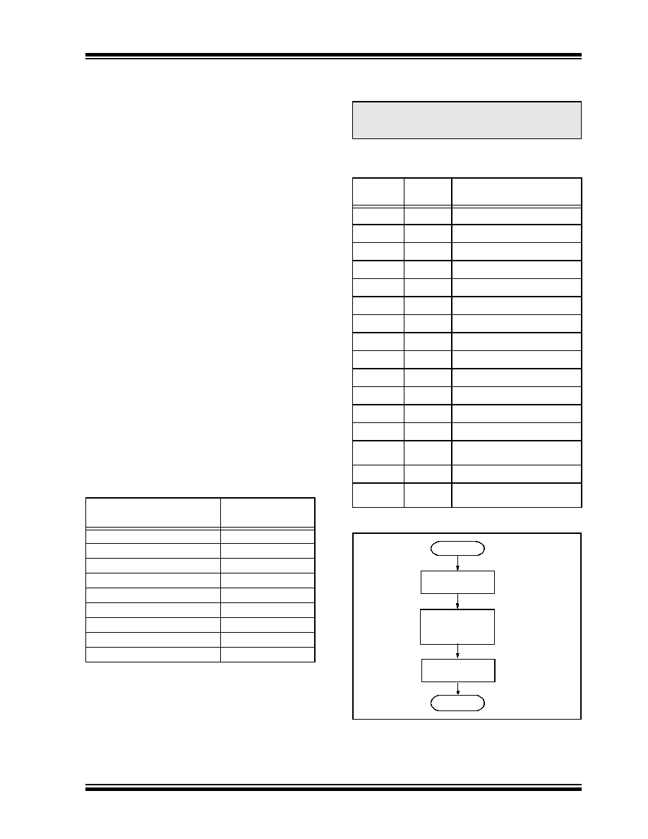
TABLE 3-1:
BULK ERASE OPTIONS
The actual Bulk Erase function is a self-timed
operation. Once the erase has started (falling edge of
the 4th PGC after the NOP command), serial execution
will cease until the erase completes (parameter P11).
During this time, PGC may continue to toggle but PGD
must be held low.
The code sequence to erase the entire device is shown
in Table 3-2 and the flowchart is shown in Figure 3-1.
TABLE 3-2:
BULK ERASE COMMAND
SEQUENCE
FIGURE 3-1:
BULK ERASE FLOW
Description
Data
(3C0005h:3C0004h)
Chip Erase
0F8Fh
Erase User ID
0088h
Erase Data EEPROM
0084h
Erase Boot Block
0081h
Erase Config Bits
0082h
Erase Code EEPROM Block 0
0180h
Erase Code EEPROM Block 1
0280h
Erase Code EEPROM Block 2
0480h
Erase Code EEPROM Block 3
0880h
Note:
A Bulk Erase is the only way to reprogram
code-protect bits from an “on” state to an
“off” state.
4-Bit
Command
Data
Payload
Core Instruction
0000
0E 3C
MOVLW 3Ch
0000
6E F8
MOVWF TBLPTRU
0000
0E 00
MOVLW 00h
0000
6E F7
MOVWF TBLPTRH
0000
0E 05
MOVLW 05h
0000
6E F6
MOVWF TBLPTRL
1100
0F 0F
Write 0Fh to 3C0005h
0000
0E 3C
MOVLW 3Ch
0000
6E F8
MOVWF TBLPTRU
0000
0E 00
MOVLW 00h
0000
6E F7
MOVWF TBLPTRH
0000
0E 04
MOVLW 04h
0000
6E F6
MOVWF TBLPTRL
1100
8F 8F
Write 8F8Fh TO 3C0004h
to erase entire device.
0000
00 00
NOP
0000
00 00
Hold PGD low until erase
completes.
Start
Done
Write 8F8Fh to
3C0004h to Erase
Entire Device
Write 0F0Fh
Delay P11 + P10
Time
to 3C0005h
相关PDF资料 |
PDF描述 |
|---|---|
| VI-271-IX-S | CONVERTER MOD DC/DC 12V 75W |
| VE-2T2-IX-S | CONVERTER MOD DC/DC 15V 75W |
| VE-27R-IX-S | CONVERTER MOD DC/DC 7.5V 75W |
| VI-25L-IX-S | CONVERTER MOD DC/DC 28V 75W |
| IDT82V2108BB | IC FRAMER T1/J1/E1 8CH 144-BGA |
相关代理商/技术参数 |
参数描述 |
|---|---|
| PIC18F24K22-E/ML | 功能描述:8位微控制器 -MCU 16KB Flash 768B RAM 8b FamilynanoWatt RoHS:否 制造商:Silicon Labs 核心:8051 处理器系列:C8051F39x 数据总线宽度:8 bit 最大时钟频率:50 MHz 程序存储器大小:16 KB 数据 RAM 大小:1 KB 片上 ADC:Yes 工作电源电压:1.8 V to 3.6 V 工作温度范围:- 40 C to + 105 C 封装 / 箱体:QFN-20 安装风格:SMD/SMT |
| PIC18F24K22-E/MV | 功能描述:8位微控制器 -MCU 16KB Flash 768B RAM 8b FamilynanoWatt RoHS:否 制造商:Silicon Labs 核心:8051 处理器系列:C8051F39x 数据总线宽度:8 bit 最大时钟频率:50 MHz 程序存储器大小:16 KB 数据 RAM 大小:1 KB 片上 ADC:Yes 工作电源电压:1.8 V to 3.6 V 工作温度范围:- 40 C to + 105 C 封装 / 箱体:QFN-20 安装风格:SMD/SMT |
| PIC18F24K22-E/SO | 功能描述:8位微控制器 -MCU 16KB Flash 768B RAM 8b FamilynanoWatt RoHS:否 制造商:Silicon Labs 核心:8051 处理器系列:C8051F39x 数据总线宽度:8 bit 最大时钟频率:50 MHz 程序存储器大小:16 KB 数据 RAM 大小:1 KB 片上 ADC:Yes 工作电源电压:1.8 V to 3.6 V 工作温度范围:- 40 C to + 105 C 封装 / 箱体:QFN-20 安装风格:SMD/SMT |
| PIC18F24K22-E/SP | 功能描述:8位微控制器 -MCU 16KB Flash 768b RAM SERIAL EE IND RoHS:否 制造商:Silicon Labs 核心:8051 处理器系列:C8051F39x 数据总线宽度:8 bit 最大时钟频率:50 MHz 程序存储器大小:16 KB 数据 RAM 大小:1 KB 片上 ADC:Yes 工作电源电压:1.8 V to 3.6 V 工作温度范围:- 40 C to + 105 C 封装 / 箱体:QFN-20 安装风格:SMD/SMT |
| PIC18F24K22-E/SS | 功能描述:8位微控制器 -MCU 16KB Flash 768B RAM 8b FamilynanoWatt RoHS:否 制造商:Silicon Labs 核心:8051 处理器系列:C8051F39x 数据总线宽度:8 bit 最大时钟频率:50 MHz 程序存储器大小:16 KB 数据 RAM 大小:1 KB 片上 ADC:Yes 工作电源电压:1.8 V to 3.6 V 工作温度范围:- 40 C to + 105 C 封装 / 箱体:QFN-20 安装风格:SMD/SMT |
发布紧急采购,3分钟左右您将得到回复。